loading
Rocket PCB  >  AI - Page Sitemap  >  stacked pcb manufacturing process hot-sale fabrication at discount
stacked pcb manufacturing process hot-sale fabrication at discount

Stacked pcb manufacturing process hot-sale fabrication at discount

Name:
10 layer ELIC printed circuit board, any layer PCB fabrication
Material:
FR4
Board thickness:
1.6mm
Surface treatment:
Immersion Gold
Technology:
Stack up N+N, Min Track/Width 3/3mil, Blind & Buried vias, laser vias
Payment:
L/C,T/T,WesternUnion
Certification:
UL Consumer (Wear, Electronic Digital, Household Appliances, Connectors)/Industrial Control/Automobile TS16949/Medical/Server, Cloud Computing & Base Station/Aviation/Military/Communication (Certification in Related Applications)
Delivery Term:
DDU, FOB, CFA, CIF, CPT, EXW
Price
Get Latest Price
Get the latest price
Quantity Needed:
Pieces
E-mail:
Product Comparison
Rocket PCB has great production capability and excellent technology. We also have comprehensive production and quality inspection equipment. printed circuit board has fine workmanship, high quality, reasonable price, good appearance, and great practicality.printed circuit board in Rocket PCB has the following advantages, compared with same kind of products in the market.
  • stacked pcb manufacturing process hot-sale fabrication at discount-Rocket PCB-img-1
    v s
    video-stacked pcb manufacturing process hot-sale fabrication at discount-Rocket PCB-img-1
Company Advantages
1. The quality of Rocket PCB HDI PCB fabrication is guaranteed. It is made by professionals who have extensive knowledge in dyeing, sewing, computer-aided design, garment construction and tailoring.
2. This product feels soft and has many other amazing qualities such as hypoallergenic material and moisture wicking & anti-microbial fabric.
3. The product is notable for high energy efficiency. When it operates, it can utilize little energy as possible without any waste.
4. With such a high aesthetic function, the product will absolutely increase the value and enhance the appeal of the houses or other buildings.
5. Our customers praise that the product has good structure strength, and it will not easily fray or rupture even our customers stretch it.


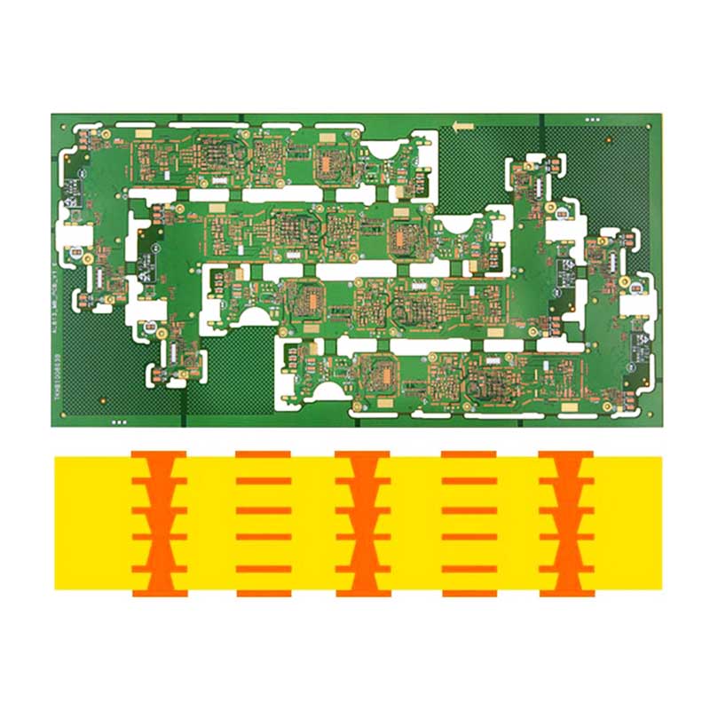
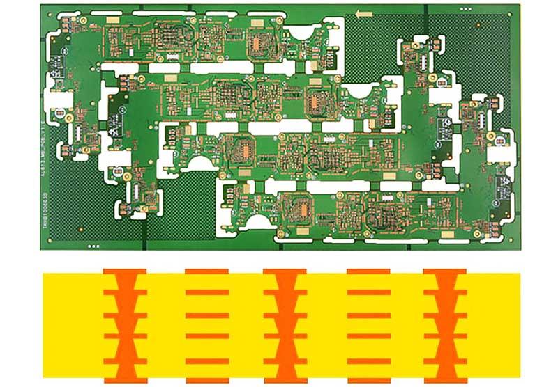
Anylayer/ ELIC (Every layer interconnection)


In order to adapt to the development of CSP and inverted chip packaging (FC), it is necessary to use high density PCB with internal via hole (IVH) structure. In order to break through the limitation of traditional HDI high density interconnection laminates, it is necessary to import higher-order any layer interconnection technology so that any layer can be arbitrarily connected to another layer to form internal conduction.

The interconnection structure of via hole (IVH)  is designed to be used in higher-level HDI products to achieve the purpose of light, thin, short and small.


stacked pcb manufacturing process hot-sale fabrication at discount-1


stacked pcb manufacturing process hot-sale fabrication at discount-2
Advantages

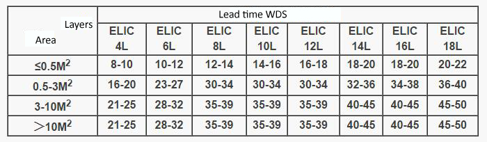
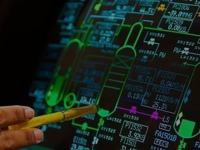
Improving high Density Wiring of Products

Reduce the weight of PCB substrate: about 60%

Reduce the size of manufactured handsets: about 30%

......


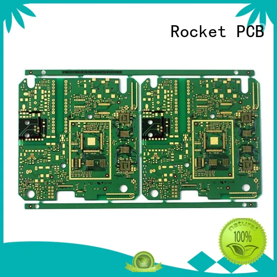
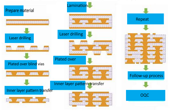
ROCKET PCB Any Layer PCB (ELIC)process flow


stacked pcb manufacturing process hot-sale fabrication at discount-3


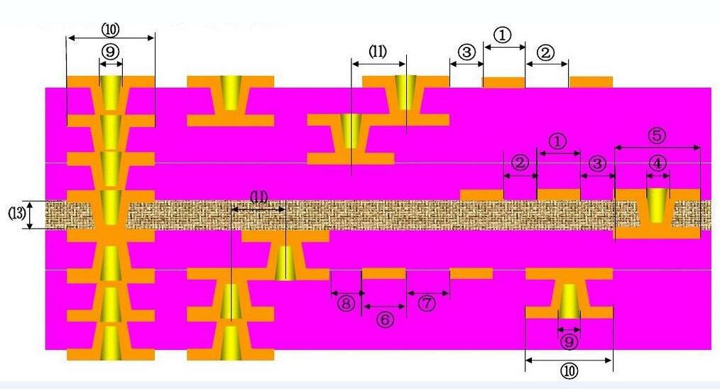
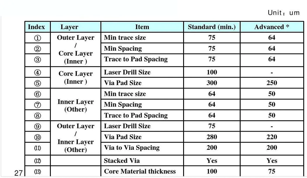
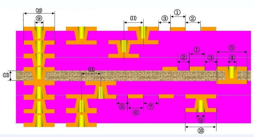
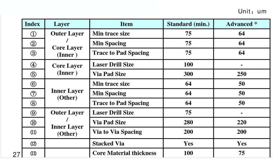
Anylayer PCB DFM suggestion for layout


stacked pcb manufacturing process hot-sale fabrication at discount-4

stacked pcb manufacturing process hot-sale fabrication at discount-5


Product FEATURES


stacked pcb manufacturing process hot-sale fabrication at discount-6

  ◪   Any Layer PCBs with laser vias and filled plating on each layer

  ◪   0.4mm thin spacing CSP supported by Any layer interconnection

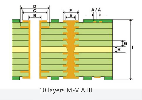
  ◪   Mass-production of 10-layer M-VIA Ⅲ (Any Layer PCB) for mobile devices

ROCKET PCB STRENGTH

stacked pcb manufacturing process hot-sale fabrication at discount-7


SPECIALIZED MANUFACTURING


  • Conductive materials and core-to-core bonding

  • Embedded components

  • RF connector attachment

  • Laser direct imaging (LDI)

  • Laser etching

  • Laser forming

  • Multi-level cavity construction

  • Plated cavities and edges

  • Composite/hybrid Structures

  • N+N dual press-fit

  • Dual-drill

  • Bonding on metal core

  • Bulid-up HDI

  • Long-short and staged gold finger

A wide range of professional manufacturing solutions, can be used for thermal energy (CTE) structural coefficients, thermal challenge design and application, extreme and unique HDI structures, and RF control

A wide range of professional manufacturing solutions, can be used for thermal energy (CTE) structural coefficients, thermal challenge design and application, extreme and unique HDI structures, and RF control

A wide range of professional manufacturing solutions, can be used for thermal energy (CTE) structural coefficients, thermal challenge design and application, extreme and unique HDI structures, and RF contro

stacked pcb manufacturing process hot-sale fabrication at discount-8


CAPABILITIES


  • 3mil line and space

  • 4mil laser defined vias

  • 6mil chip-on-board

  • 6mil mechanically drilled vias

  • Conductive and non-conductive via fill

  • Dual backdrilling

  • Sequential lamination

  • Mixed dielectric

  • Heatsink Bonding

  • Heavy copper/thermal vias

  • Blind/buried vias

  • Stacked and staggerd microvias


stacked pcb manufacturing process hot-sale fabrication at discount-9

EXTENSIVE ANALYTICAL TESTINGstacked pcb manufacturing process hot-sale fabrication at discount-10


  • Design Rules Check(DRC)

  • Electrical Testing

  • Automated Optical Inspection(AOI)

  • X-Ray

  • Plating thickness testing

  • Metalized vias inspection

  • Thermal shock testing

  • Surface peelability testing

  • Impedance control testing

  • 100% visual inspection

  • Solderability testing

  • Ionic cleanliness testing

  • Metallographic microscopic analysis

  • High voltage testing

  • Insulating resistance testing


stacked pcb manufacturing process hot-sale fabrication at discount-11


FEATURES


  • PTFE

  • High speed/low loss

  • High temperature

  • Low CTE

  • Lead-free, HASL, ENIG, EPENIG, Immersion Silver, Tin, Gold finger

  • Combination surface finished

  • Copper-filled microvias


Product application


stacked pcb manufacturing process hot-sale fabrication at discount-12                
Consumer electronics
stacked pcb manufacturing process hot-sale fabrication at discount-13                
Automotive electronics
stacked pcb manufacturing process hot-sale fabrication at discount-14                
Communications
stacked pcb manufacturing process hot-sale fabrication at discount-15                
Energy
stacked pcb manufacturing process hot-sale fabrication at discount-16                
Industrial & Instrumentation
stacked pcb manufacturing process hot-sale fabrication at discount-17                
IOT/Smart Home
stacked pcb manufacturing process hot-sale fabrication at discount-18                
Medical electronics
stacked pcb manufacturing process hot-sale fabrication at discount-19                
Security Industry

Company Features
1. Rocket PCB Solution Ltd. is the leading manufacturer of pcb manufacturing process with advanced production machines.
2. Rocket PCB attaches great importance to forward-looking technology applications in the production of any-layer pcb .
3. Rocket PCB Solution Ltd. has made full preparation to meet up with all victories or challenges. Call now! Rocket PCB Solution Ltd. is professional and loyal to exceeding our customer's vision. Call now! It is Rocket PCB Solution Ltd.'s goal to seek the excellent quality. Call now! To be one of the advanced double layer pcb manufacturer is the hope of Rocket PCB. Call now!
Thanks to the low cost of raw materials and the high efficiency of streamlined production, double layer pcb products have the advantage of high gross profit margin. Its components are always soldered in, which contributes to durability
Rocket PCB double layer pcb comes in a variety of wonderful designs. Its assembly process is conducted by a computer, leaving very little room for error
High technical assurance and first-class quality can be seen on pcb manufacturing process. It improves the wiring density and reduces the spacing of components
All raw materials used to manufactured Rocket PCB HDI PCB fabrication have to go through stringent quality checking procedure. Its connections made automatically through copper tracks
The design of Rocket PCB any-layer pcb focuses on the technique and function.
any-layer pcb has advantages both in cost, reliability and long life, in comparison with other similar products. It makes the interconnections less bulky
Product Message
Chat Online
Chat Online
Leave Your Message inputting...
Thank you for your attention. Please kindly describe your question first, or please send your inquiry to our email sales@rocket-pcb.com, and we will reply to you ASAP. Welcome, what can I help you?
Sign in with: