loading
Rocket PCB  >  AI - Page Sitemap  >  stacked double layer pcb free sample precision at discount
stacked double layer pcb free sample precision at discount

Stacked double layer pcb free sample precision at discount

Name:
10 layer ELIC printed circuit board, any layer PCB fabrication
Material:
FR4
Board thickness:
1.6mm
Surface treatment:
Immersion Gold
Technology:
Stack up N+N, Min Track/Width 3/3mil, Blind & Buried vias, laser vias
Payment:
L/C,T/T,WesternUnion
Certification:
UL Consumer (Wear, Electronic Digital, Household Appliances, Connectors)/Industrial Control/Automobile TS16949/Medical/Server, Cloud Computing & Base Station/Aviation/Military/Communication (Certification in Related Applications)
Delivery Term:
DDU, FOB, CFA, CIF, CPT, EXW
Price
Get Latest Price
Get the latest price
Quantity Needed:
Pieces
E-mail:
Company Advantages
1. The main components of double layer pcb are made from imported materials. It takes less time in assembling a circuit as compared to the conventional method
2. Over the years in the market, this product has received no complaints from our customers. It is hard to find any short circuits in this product
3. The product is extremely ergonomic. Its ergonomic shape of hugs the natural curve of the back distributing the weight evenly. It offers a simple platform to arrange the electronic components in a compressed way
4. The product will not contaminate the food during the dehydration. There is a defrosting tray to collect the water vapor which may drop to the food. Thanks to the application of the shielding layer, its signal distortion is reduced
5. The product has a superior appearance. It is innovatively designed with visual impact and has a high-gloss finish that is provided by RTM technology.


Anylayer/ ELIC (Every layer interconnection)


In order to adapt to the development of CSP and inverted chip packaging (FC), it is necessary to use high density PCB with internal via hole (IVH) structure. In order to break through the limitation of traditional HDI high density interconnection laminates, it is necessary to import higher-order any layer interconnection technology so that any layer can be arbitrarily connected to another layer to form internal conduction.

The interconnection structure of via hole (IVH)  is designed to be used in higher-level HDI products to achieve the purpose of light, thin, short and small.


stacked double layer pcb free sample precision at discount-1


stacked double layer pcb free sample precision at discount-2
Advantages

Improving high Density Wiring of Products

Reduce the weight of PCB substrate: about 60%

Reduce the size of manufactured handsets: about 30%

......


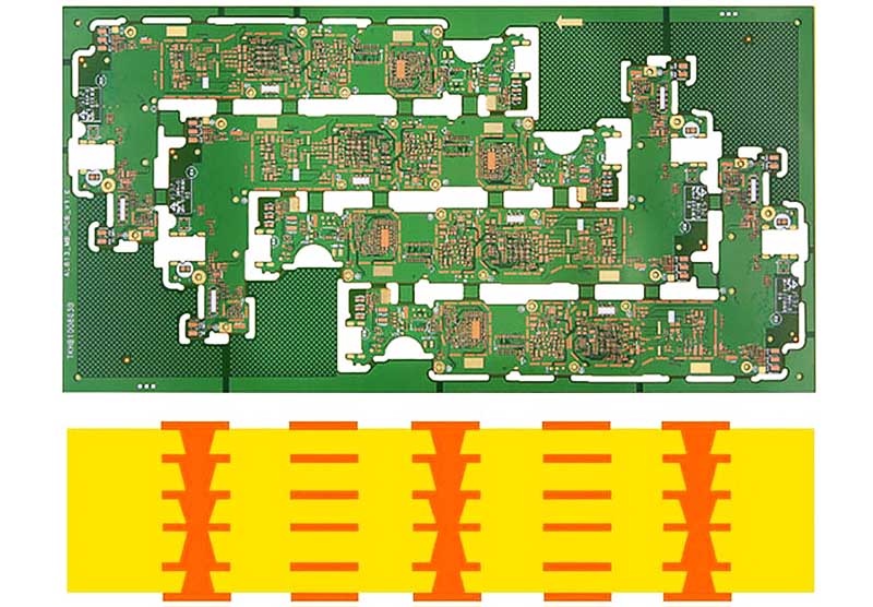
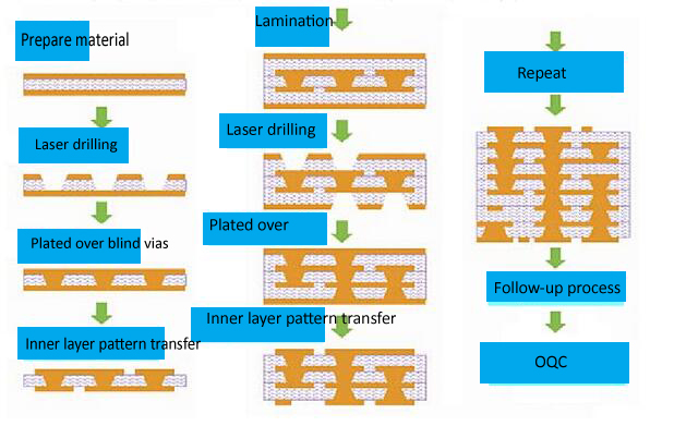
ROCKET PCB Any Layer PCB (ELIC)process flow


stacked double layer pcb free sample precision at discount-3


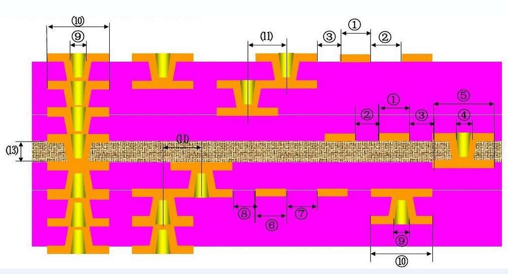
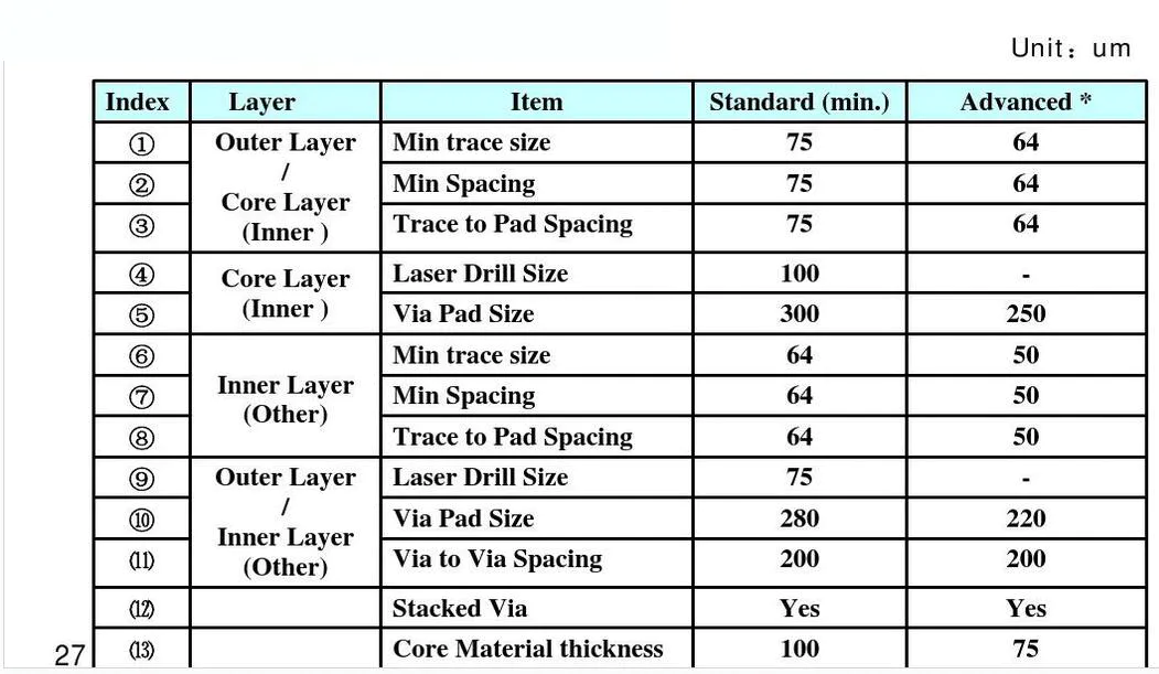
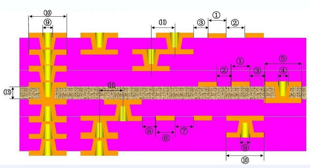
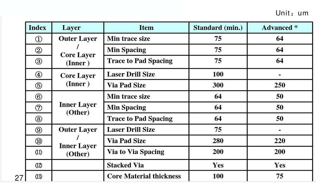
Anylayer PCB DFM suggestion for layout


stacked double layer pcb free sample precision at discount-4

stacked double layer pcb free sample precision at discount-5


Product FEATURES


stacked double layer pcb free sample precision at discount-6

  ◪   Any Layer PCBs with laser vias and filled plating on each layer

  ◪   0.4mm thin spacing CSP supported by Any layer interconnection

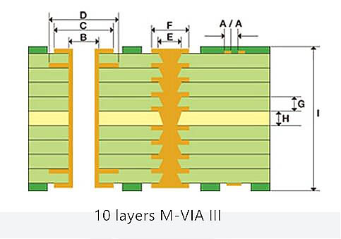
  ◪   Mass-production of 10-layer M-VIA Ⅲ (Any Layer PCB) for mobile devices


The technology of making any layer HDI is summarized as follows


1) Precision alignment technology is one of the key technologies in making any-layer HDI board. In order to achieve precise inter-layer alignment effect, scientific and reasonable alignment target design and alignment mode are prerequisites.

2) All factors affecting the expansion, shrinkage and deformation of any layer HDI board need to be eliminated as far as possible. Precise inter-layer alignment effect of any layer HDI board will be affected by pre-placement of core board, plate selection, equipment difference and operation control.

3) Precision alignment technology is a control technology that runs through the whole process of making any- layer HDI board. It has very high requirements for equipment, materials, process parameters, personnel operation and production environment.


With the development of PCB towards light, thin, short, small and high reliability, the requirement of interlayer alignment accuracy for any layer HDI boards will bring more challenges and higher requirements for existing interlayer alignment control technology. In order to solve the problem of alignment accuracy of any layer HDI board, it is necessary to make a thorough study on it, make a comprehensive and detailed analysis from the technical principle to the actual operation, and find out the factors that affect the alignment accuracy to eliminate or decrease one by one. So that our inter-layer precise alignment technology is more mature, its control is more scientific, systematic and standardized, to meet the current production needs of higher-end PCB, to seize more market opportunities.


Product application


stacked double layer pcb free sample precision at discount-7                
Consumer electronics
stacked double layer pcb free sample precision at discount-8                
Automotive electronics
stacked double layer pcb free sample precision at discount-9                
Communications
stacked double layer pcb free sample precision at discount-10                
Energy
stacked double layer pcb free sample precision at discount-11                
Industrial & Instrumentation
stacked double layer pcb free sample precision at discount-12                
IOT/Smart Home
stacked double layer pcb free sample precision at discount-13                
Medical electronics
stacked double layer pcb free sample precision at discount-14                
Security Industry

Company Features
1. Rocket PCB Solution Ltd.'s production of double layer pcb is in the leading position nationwide.
2. Rocket PCB Solution Ltd. has strong financial, professional and technical strength.
3. Our value is: we accept personal responsibility for our actions and focus on finding solutions and delivering results. We keep our promises and commitments.
The raw materials of Rocket PCB double layer pcb are paid great attention during the incoming material inspections. The product has the advantage of high strength
Rocket PCB double layer pcb is manufactured with raw materials that meet the regulatory specification. It receives popularity among customers from Europe, America, Middle East, and so on
The design of Rocket PCB double layer pcb is simple but practical. It receives popularity among customers from Europe, America, Middle East, and so on
Rocket PCB double layer pcb is superior with reliable material and advanced process. It can withstand the corrosion of acid, alkali, and other chemical substances
Rocket PCB double layer pcb is designed and manufactured by a team of skilled employees. The product is widely accepted for its abrasion resistance
The quality of the product is under the guarantee of international certificates. Through hardening treatment, it is sturdy enough
Product Message
Chat Online
Chat Online
Leave Your Message inputting...
Thank you for your attention. Please kindly describe your question first, or please send your inquiry to our email sales@rocket-pcb.com, and we will reply to you ASAP. Welcome, what can I help you?
Sign in with: