loading
Rocket PCB  >  AI - Page Sitemap  >  stacked custom circuit board manufacturers free sample layer
stacked custom circuit board manufacturers free sample layer

Stacked custom circuit board manufacturers free sample layer

Name:
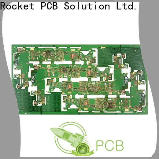
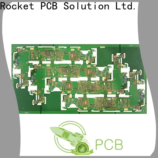
10 layer ELIC printed circuit board, any layer PCB fabrication
Material:
FR4
Board thickness:
1.6mm
Surface treatment:
Immersion Gold
Technology:
Stack up N+N, Min Track/Width 3/3mil, Blind & Buried vias, laser vias
Payment:
L/C,T/T,WesternUnion
Certification:
UL Consumer (Wear, Electronic Digital, Household Appliances, Connectors)/Industrial Control/Automobile TS16949/Medical/Server, Cloud Computing & Base Station/Aviation/Military/Communication (Certification in Related Applications)
Delivery Term:
DDU, FOB, CFA, CIF, CPT, EXW
Price
Get Latest Price
Get the latest price
Quantity Needed:
Pieces
E-mail:


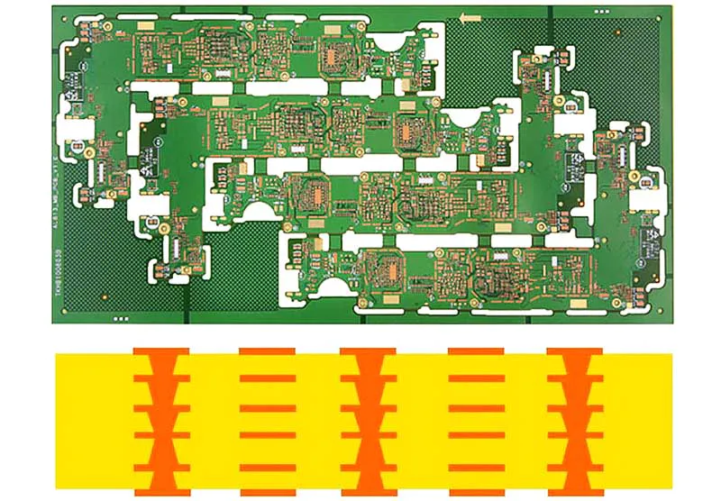
Anylayer/ ELIC (Every layer interconnection)


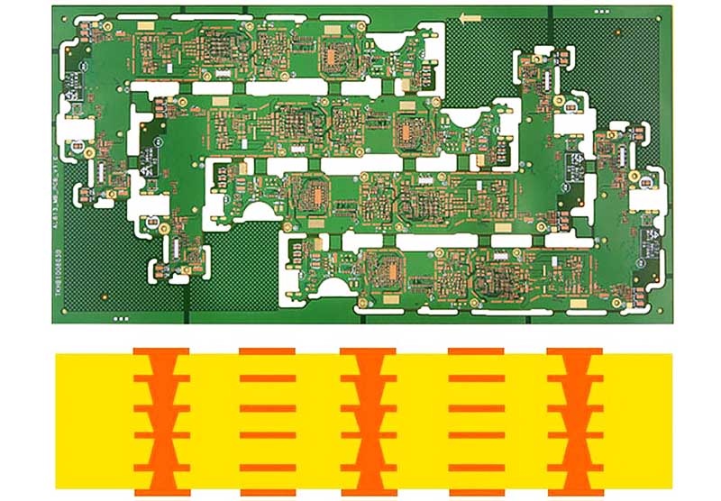
In order to adapt to the development of CSP and inverted chip packaging (FC), it is necessary to use high density PCB with internal via hole (IVH) structure. In order to break through the limitation of traditional HDI high density interconnection laminates, it is necessary to import higher-order any layer interconnection technology so that any layer can be arbitrarily connected to another layer to form internal conduction.

The interconnection structure of via hole (IVH)  is designed to be used in higher-level HDI products to achieve the purpose of light, thin, short and small.
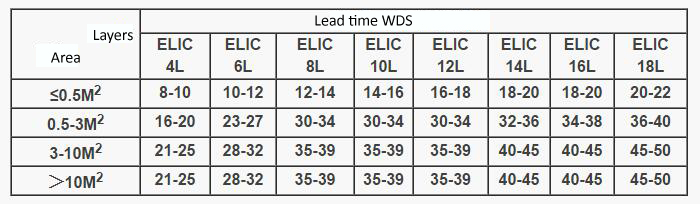

stacked custom circuit board manufacturers free sample layer-1


stacked custom circuit board manufacturers free sample layer-2
Advantages

Improving high Density Wiring of Products

Reduce the weight of PCB substrate: about 60%

Reduce the size of manufactured handsets: about 30%

......


ROCKET PCB Any Layer PCB (ELIC)process flow
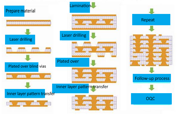


stacked custom circuit board manufacturers free sample layer-3


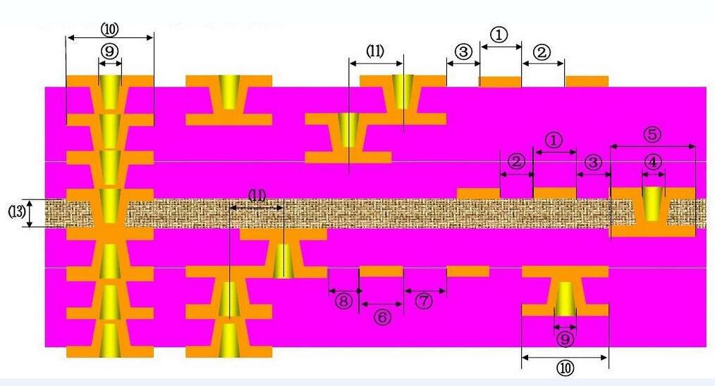
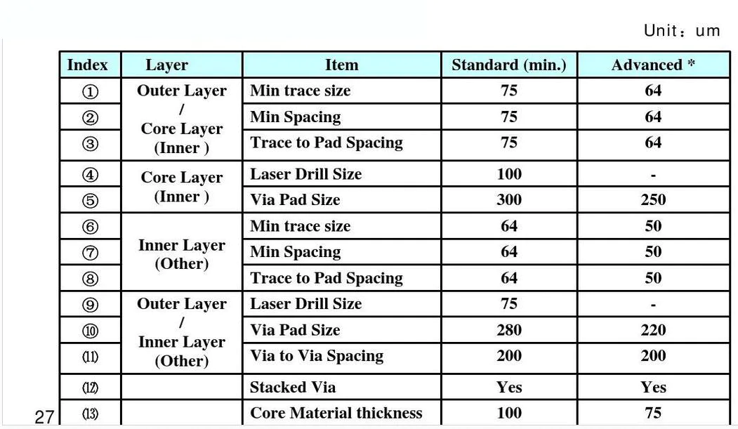
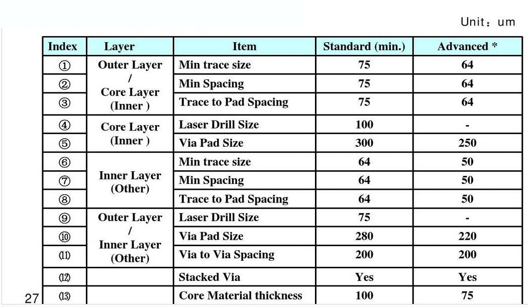
Anylayer PCB DFM suggestion for layout
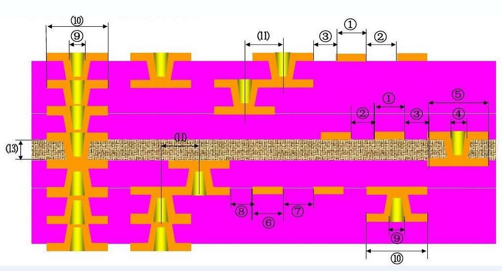

stacked custom circuit board manufacturers free sample layer-4

stacked custom circuit board manufacturers free sample layer-5


Product FEATURES


stacked custom circuit board manufacturers free sample layer-6

  ◪   Any Layer PCBs with laser vias and filled plating on each layer

  ◪   0.4mm thin spacing CSP supported by Any layer interconnection

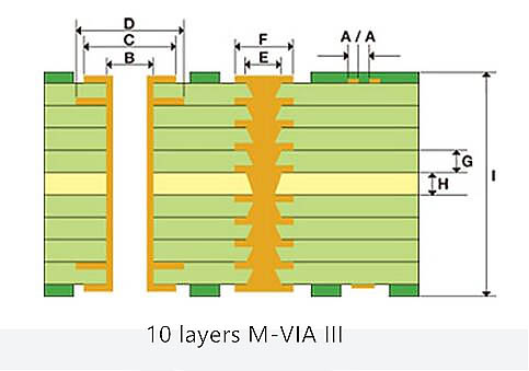
  ◪   Mass-production of 10-layer M-VIA Ⅲ (Any Layer PCB) for mobile devices


The technology of making any layer HDI is summarized as follows


1) Precision alignment technology is one of the key technologies in making any-layer HDI board. In order to achieve precise inter-layer alignment effect, scientific and reasonable alignment target design and alignment mode are prerequisites.

2) All factors affecting the expansion, shrinkage and deformation of any layer HDI board need to be eliminated as far as possible. Precise inter-layer alignment effect of any layer HDI board will be affected by pre-placement of core board, plate selection, equipment difference and operation control.

3) Precision alignment technology is a control technology that runs through the whole process of making any- layer HDI board. It has very high requirements for equipment, materials, process parameters, personnel operation and production environment.


With the development of PCB towards light, thin, short, small and high reliability, the requirement of interlayer alignment accuracy for any layer HDI boards will bring more challenges and higher requirements for existing interlayer alignment control technology. In order to solve the problem of alignment accuracy of any layer HDI board, it is necessary to make a thorough study on it, make a comprehensive and detailed analysis from the technical principle to the actual operation, and find out the factors that affect the alignment accuracy to eliminate or decrease one by one. So that our inter-layer precise alignment technology is more mature, its control is more scientific, systematic and standardized, to meet the current production needs of higher-end PCB, to seize more market opportunities.




Product application


stacked custom circuit board manufacturers free sample layer-7                
Consumer electronics
stacked custom circuit board manufacturers free sample layer-8                
Automotive electronics
stacked custom circuit board manufacturers free sample layer-9                
Communications
stacked custom circuit board manufacturers free sample layer-10                
Energy
stacked custom circuit board manufacturers free sample layer-11                
Industrial & Instrumentation
stacked custom circuit board manufacturers free sample layer-12                
IOT/Smart Home
stacked custom circuit board manufacturers free sample layer-13                
Medical electronics
stacked custom circuit board manufacturers free sample layer-14                
Security Industry

Each Rocket PCB custom circuit board manufacturers is made very durable with only the best quality components. It is tested to deal with extreme fluctuations in temperature, especially summer. The thermal printing method adopted in this product helps reduce printing cost because it needs no ink
The law of heat conduction theory has been adopted in the developing of Rocket PCB custom circuit board manufacturers. It's specially made to allow the heat to be transferred from the higher temperature region to the lower temperature region. It is less likely to occur the paper jamming problem
Before the Rocket PCB custom circuit board manufacturers is stored or shipped, the finishing operations and inspection remain to be performed following curing. The finishing operation trims flash or excess rubber. Printing error is less likely to happen, leading to less downtime for this product
The quality of Rocket PCB custom circuit board manufacturers meets the National Sanitation Foundation recommendations for water purifiers. Each production stage will be scrutinized to guarantee its quality. This product produces clear images or characters
During the designing stage of Rocket PCB custom circuit board manufacturers, the designers will carry out a water test based on this product with the aim to pick out the right treatment system to remove different particulates. The thermal printing method adopted in this product helps reduce printing cost because it needs no ink
With a properly laid out electrical circuits and finely arranged components, this product is not subject to noises, such as noise caused by loose connection of components. Without the capacity need for ribbons and ink, its design is more compact
Product Message
Chat Online
Chat Online
Leave Your Message inputting...
Thank you for your attention. Please kindly describe your question first, or please send your inquiry to our email sales@sllpcb.com, and we will reply to you ASAP. Welcome, what can I help you?
Sign in with: