multilayer printed circuit boards: how are they made and what are they good for
by:Rocket PCB
2019-09-24
Multi-person PCB (
Printed circuit board)
Consists of two or more printed circuit boards stacked together to establish a reliable mutual connection between them.
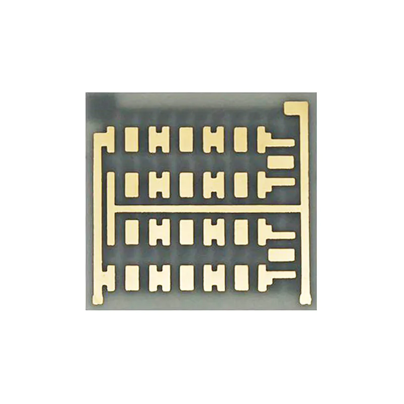
Multi-layer pcb has at least three layers of conductive layer.
Two layers of outer and middle layers synthesized and encapsulated by outer insulation.
Due to the complex manufacturing method, the production of multi-layer PCB is very unique and the price is very high.
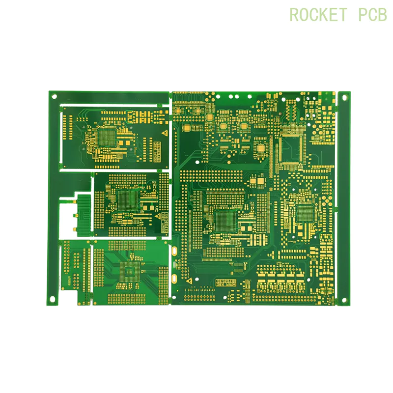
The pcb of the basic electronic equipment includes 4 to 8 layers, while the pcb of the more complex equipment can have 8 to 40 layers.
In a PCB, the number of layers on a multi-layer PCB is recognized as the number of independent conductor patterns.
This is usually an even number, including two outer layers.
Engineers/designers create layouts using computer-aided design (CAD system)
It uses its own internal data format and then extends to the Gerber file.
The Gerber file provides information on the required copper tracking layers, as well as solder joints of the board and all other options.
After the designer confirms, create the photo tool using the photo drawing machine that ultimately provides the image for the pcb.
This picture enables the machine to print the inner layer in the right way with epoxy and laminate.
It also includes fiberglass, which has copper foil pre-
Glue on each side of the resin.
Later, a powerful alkaline solution was used to dissolve or dissolve the internal layer to remove unwanted copper as needed.
This makes the internal core area of the multi-layer PCB complete.
Later, the required holes are punched to satisfy and arrange the inner layer to the outer layer.
This process is called Register punching and (AOI)
Automatic optical detection.
When the required holes are created, all layers are assembled together and then the drill holes of the PCB are started.
The holes of the lead component are drilled, and also by holes that connect the copper layer together.
To find the target hole, use X-
Ray drill was used.
The next stage involves plating by applying a chemical deposition of a very thin layer of copper to cover the inside of the drill.
Prior to this, the external layer is imaged to ensure that there is no short circuit in the circuit board.
Later, the board was plated with copper.
Check them to make sure the electrical connection is good.
After that, the outer layer dissolves or removes the excess and unwanted copper.
To ensure that the required copper is not damaged, the surface area is coated with tin as a protective barrier.
Later, a welding mask is printed on each side of the board to protect the copper surface.
This is also to prevent short welding
A short circuit occurs during assembly.
All multi-layer boards are electrically tested using a flight probe tester to ensure that there are no open or faulty areas.
Finally, the pcb is cut off according to the needs of the customer.
Every step of PCB manufacturing has to be handled very carefully by experts, which is why you should only choose a professional PCB manufacturing company such as Super PCB.
A rigid and flexible pcb is specially provided and services are provided.
Printed circuit board)
Consists of two or more printed circuit boards stacked together to establish a reliable mutual connection between them.
Multi-layer pcb has at least three layers of conductive layer.
Two layers of outer and middle layers synthesized and encapsulated by outer insulation.
Due to the complex manufacturing method, the production of multi-layer PCB is very unique and the price is very high.
The pcb of the basic electronic equipment includes 4 to 8 layers, while the pcb of the more complex equipment can have 8 to 40 layers.
In a PCB, the number of layers on a multi-layer PCB is recognized as the number of independent conductor patterns.
This is usually an even number, including two outer layers.
Engineers/designers create layouts using computer-aided design (CAD system)
It uses its own internal data format and then extends to the Gerber file.
The Gerber file provides information on the required copper tracking layers, as well as solder joints of the board and all other options.
After the designer confirms, create the photo tool using the photo drawing machine that ultimately provides the image for the pcb.
This picture enables the machine to print the inner layer in the right way with epoxy and laminate.
It also includes fiberglass, which has copper foil pre-
Glue on each side of the resin.
Later, a powerful alkaline solution was used to dissolve or dissolve the internal layer to remove unwanted copper as needed.
This makes the internal core area of the multi-layer PCB complete.
Later, the required holes are punched to satisfy and arrange the inner layer to the outer layer.
This process is called Register punching and (AOI)
Automatic optical detection.
When the required holes are created, all layers are assembled together and then the drill holes of the PCB are started.
The holes of the lead component are drilled, and also by holes that connect the copper layer together.
To find the target hole, use X-
Ray drill was used.
The next stage involves plating by applying a chemical deposition of a very thin layer of copper to cover the inside of the drill.
Prior to this, the external layer is imaged to ensure that there is no short circuit in the circuit board.
Later, the board was plated with copper.
Check them to make sure the electrical connection is good.
After that, the outer layer dissolves or removes the excess and unwanted copper.
To ensure that the required copper is not damaged, the surface area is coated with tin as a protective barrier.
Later, a welding mask is printed on each side of the board to protect the copper surface.
This is also to prevent short welding
A short circuit occurs during assembly.
All multi-layer boards are electrically tested using a flight probe tester to ensure that there are no open or faulty areas.
Finally, the pcb is cut off according to the needs of the customer.
Every step of PCB manufacturing has to be handled very carefully by experts, which is why you should only choose a professional PCB manufacturing company such as Super PCB.
A rigid and flexible pcb is specially provided and services are provided.
Custom message