
Related Products
English


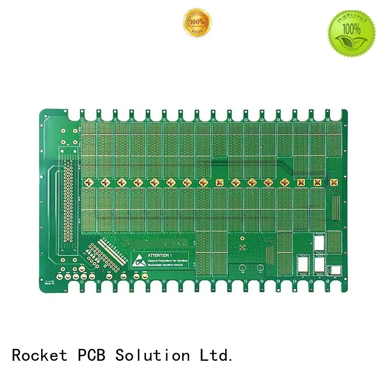


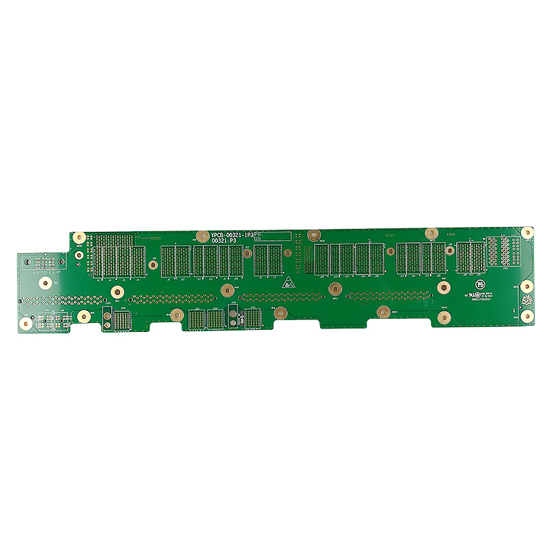
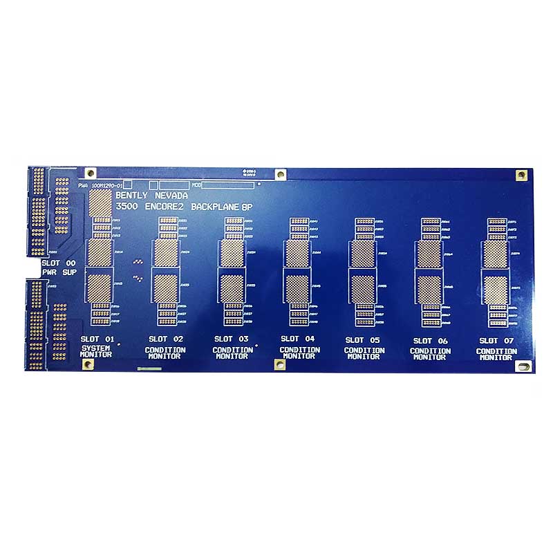
PCB Backplane Technology
The backplane has always been a
specialized product in the PCB manufacturing industry, the backplane is
thicker and heavier than the conventional PCB board, and its heat
capacity is larger accordingly.
In
view of the slow cooling speed of the backplane, the length of the
reflow weld furnace should be lengthened. There is also a need for
forced air cooling at the outlet to reduce the backplane temperature to a
safe operating level.
The user's need for thinner cores and more layers of backplane comes to the opposite requirements of the conveyor system. When a large power application card is plugged into the backplane, the copper layer thickness must be moderate to provide the required current,all of these factors lead to an increase in the average weight of the backplane. This requires that conveyor belts and other conveyor systems must not only be able to safely transfer large-size raw material backplanes, and it must also be taken the weight increment into account.
Because the backplane is thicker than the conventional PCB, and the number of holes is much more, it is easy to cause the outflow phenomenon of processing fluid. In order to minimize the amount of liquid carrying and remove the possibility of any impurities remaining at the through hole, it is very important to clean the hole by means of high-pressure flushing and air blower.
Interlayer alignment become important due to the increasing number of layers required by user applications. Interlayer-to-bit requirements tolerance convergence, larger backplane size makes this convergence more demanding.
All pattern processes are produced in a controlled environment of a certain temperature and humidity. The alignment tolerance of the entire area before and after the graph should be maintained at 0.0125mm. CCD camera needs to be used to complete the front and rear layout of the position. After etching, use four drilling system to perforated the inner laminates. Perforated through the core board, position accuracy maintained at 0.025mm, the repeatable capacity of 0.0125mm, then insert the perforation with the pin, align the etched inner layer, At the same time glue the inner layer together. The use of this etched perforation method can fully ensure that the hole and etching copper plate alignment, forming a solid ring design structure. However, with the user in the PCB wiring requirements more detailed, in order to keep the board cost unchanged, the etching copper plate size is required to be smaller, thus requiring better alignment of the interlayer copper plate. Fixture and conveyor equipment must be able to transmit large plates and heavy plates simultaneously.
In addition to drilling requirements, backplane designers generally
have different requirements for copper uniformity on the surface of the
outer layer Some designs etch very few signal lines on the outer layer.
On the other hand, in the face of high-speed data rate and impedance
control line requirements, the external layer set solid copper sheet
will become very necessary for the use of EMC shielding layer
Etching
line widths, thicknesses, and tolerances become key indicators for the
effectiveness and repeatable control of the backplane impedance. At this
point, the AOI method can be used to ensure that the etched copper
pattern matches the design data. The impedance model is used to
determine and control the sensitivity of the impedance to the line width
change by setting the line width tolerance on the AOI.
Traditionally, for reliability reasons, there is a tendency to use passive components on the Backplane. However, in order to maintain the fixed cost of active plate, BGA and other active devices are more and more designed on the Backplane, component mounting equipment must not only be able to place smaller specifications of capacitors and resistors but also be able to operate on additional silicon packaging components. In addition, the Backplane large specification requires the installation of equipment bed to be large, and the heavy backplane can also be shifted with fine position tolerances.
The quality of raw materials is not up to standard
The quality of raw materials is the basic quality of circuit boards. The material itself is not up to standard. The circuit boards made will appear foaming, stratification, board warping and uneven thickness.
Production equipment is not up to standard
With the progress of science and technology, the replacement of PCB production equipment is faster and faster, and the price is more and more expensive. Equipment is to ensure the quality of hardware, increase investment in equipment, so that equipment to achieve high efficiency, stability is the fundamental way to improve the quality of circuit boards. As a result, some small PCB factories are unable to purchase expensive equipment, which ultimately leads to the poor quality of products.
Production technology is not up to standard
Each process of PCB production must be carried out in accordance with strict production process, and each process must be equipped with corresponding inspection equipment. These process parameters and equipment can guarantee the stability of PCB quality. Because the production technology is not up to the standard, many PCB factories only have low prices, resulting in the quality of the production line board is not up to standard.
The first point is the circuit design
The PCB with good quality must have reasonable circuit design. Whether double-layer or multi-layer board, it must have accurate line control and reasonable trace trend, in order to avoid the slow response due to redundant lines, that is, line width, line thickness, line spacing meet the requirements, so as to avoid line heating, circuit breakage, and short circuit.
The second point is the appearance
The PCB circuit board with good quality not only has a neat and smooth surface, but also basically does not appear the phenomenon of bending or uneven. The copper surface is not easy to oxidize, and there will be no cracks or scars, ink falling off.
The third point is the heat resistance of the product
This point should be observed personally, PCB circuit boards are assembled in their own products. If they can withstand the instantaneous high temperature produced by welding and the copper foil is not easy to fall off under high temperature, it shows that the PCB circuit boards have good heat resistance and good quality.
The fourth point is the expansion coefficient
PCB circuit boards can produce drastic expansion or contraction in hot and cold environment. If the expansion coefficient is small and the thermal and cold environment has little influence on PCB circuit boards, the quality of PCB circuit boards is good and the components on PCB circuit boards will not be damaged.
Yield Advantages
Strong fabrication strength, can meet the bulk needs of different clients
> The factory invested heavily in importing foreign advanced PCB production equipment, such as Burkle laminator, Mitsubishi laser drill, Hitachi mechanical drill, Japan screen automatic exposure machine, LDI, AOI etc, highly automated production.With a monthly output of up to 250,000 square meters.
> Our suppliers have formed a complete production process, which is becoming more specialized, modern and large-scale, has signed long-term strategic cooperation agreements with well-known enterprises at home and abroad.
> Our superb quality and leading market position are guaranteed under the ISO9001, ISO14001, ISO/TS16949, OHSAS18001, ISO/IEC27001, UL, SGS, ROHS system with our strong technical development drive. We also insist on adopting 5S methods, Lean and Six Sigma quality systems.
Technical Advantages
> We provide real-time and in-depth technical support. Tailor-made application solutions, like high speed, high capacity and high frequency, press-fit, heat-sink solutions.
> Free DRC and DFM
> Rapid feedback on the layout,build-up, panels, impedance, material selection, design rules, manufacturability, costs of different solutions, use of micro vias, gold plating, special laminates, etc.We always put the best interests first when providing innovative solutions for manufacturing customers’ products
> Rocket provides industry-leading support to our customers so that we can help them grow
Advanced Product and Advanced Technology
Service Advantages
> 24 hours online tech support and fast quote in 2 hours for standard board
> A number of production lines meet the request of mass production and fast turn around of small batches and various prototype PCBs
> Expedited production line for prototyping double-sided PCB up to 24 hours, 4 layers 48 hours, 6 layers 72 hours etc.
> Mass production of double-sided PCB 5-6 days lead time, multi-layer PCB 7-9 days.
> DHL, Fedex, TNT, UPS Express delivery, fully meet the customer's time requirements, on time delivery more than 99%

> Strict production and testing, 100% outgoing pass rate.
> Provide 1-64 layers of different thickness, different materials, different processes of product customization, of which the CCL using A-class raw materials, high quality assurance.
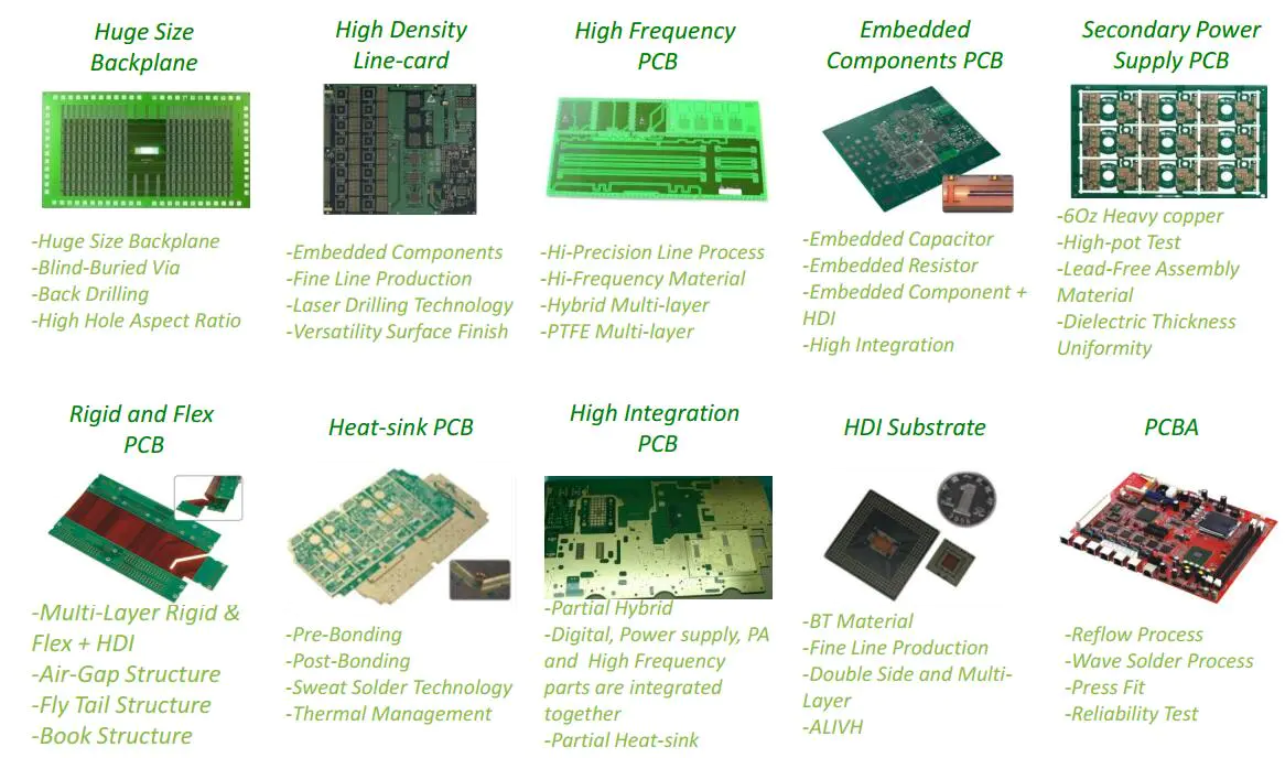
> Unlimited PCB capabilities,we provide various and advanced technology PCBs include rigid, FPC, rigid-flex, metal core, microwave/RF, HDI, any layer, heavy copper, large-size, embedded, LED, backplane, ceramic substrate, IC substrate, high-frequency, high-density and high-performance PCB.
> Eight major surface treatment technology and high-quality ink printing, beautiful and reliable.
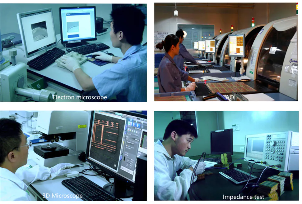
> Dozens of tests such as open/short circuit testing( ET test), AOI, X-ray, impedance testing, solderability testing, thermal shock testing, metallographic micro-slicing analysis, halogen-free testing, etc.
◪ Panel sizes up to 54 inches
◪ Over 70 layers
◪ Blind and back drilled through holes
◪ Dual diameter holes
◪ Heavy copper layers
◪ Connector expertise
◪ 24 hour real-time technical support Quick turn around with 24 hours and instant quote. For HDI board, will be based on board parameters, normally 15-30 days.
◪ Effective and flexible PCB engineering solutions save your cost. We always put
the best interests first when providing innovative solutions for
manufacturing customers’ products,we are more willing to help customers grow.
◪ Rapid feedback on the layout,build-up, panels,
impedance, material selection, design rules, manufacturability,
costs of different solutions, use of micro vias, gold plating, special
laminates, etc.
◪ Strong partnerships with different reputed material suppliers such as
Rogers, Arlon, Nelco and Taconic can realize a fast service to a wide
range of PCB applications.
◪ Dozens of tests such as open/short
circuit testing( ET test), AOI, X-ray, impedance testing, solderability
testing, thermal shock testing, metallographic micro-slicing analysis,
halogen-free testing, etc.100% outgoing pass rate.
◪ Complete services from free DFM, traceable manufacturing to complete after-sales service, on time delivery 99%.
◪ We will keep secret for customer sale area,design ideas, drawing and all other private information.
◪ Flexible payment terms. Samples for 100%TT, mass production payment: 50% advance payment 50% balance should be paid off before loading or accept monthly statement if the order is stable.


Quick Links
About Us
Contact Us
Tel:(+86) 158 9965 5195
Office:(+86) 755 23040566
E-mail:sales@sllpcb.com
Microsoft Teams:hank_168
WhatsApp:+86 186 0723 3179
Office Address:2207,Bid 4,He Gu Shan Hui Cheng,35#,Guang Tian Ro Yanluo street, Song Gang Town,518105 SHENZHEN, CHINA
Plant ADD: No 69, Lianfeng North Road, Xianxi Area, ChangAn Town, Dongguan, China.


