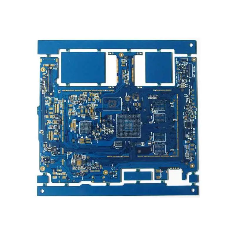
Why need to high density circuit board
Traditional circuit boards are often divided into single-sided PCB, double-sided circuit boards, PCB sandwich plate, and the PCB sandwich plate is divided into single pressing and bonding structure many times. This design involves some electrical properties and link density problem, of course, but because the technology of electronic products to develop fast, the geometric structure can meet the demand of installation of density and electrical components. In order to improve the component link density, from geometric point of view only compression lines and connection point space, can accommodate more contact improve link density in small space. , of course, also can be in multiple component stack to a position, to enhance the astral dimension. So high density circuit board is not simply a kind of circuit board technology, as well as electronic packaging and assembly issue. Links in order to improve the element density, from geometric point of view only compression lines and connection points of space, let more contact to accommodate in a smaller space, to improve the link density. Of course have a different idea, that is to a number of different components can be stacked in the same position, in order to improve the density of construct. So from a certain perspective, high density circuit board is not just a circuit board technology, is also a problem with assembly, electronic packaging that is worth industry makes some efforts to understand, I'm afraid. PCB laminated general electronic packaging, refers to the semiconductor wafer and link relation between the load board, road board association in this area is 'electronic structure loading plate technology' a book published, interested can refer to. As for electronic assembly parts, is again after the completion of the electronic packaging components installed in another piece of work function circuit boards. This aspect of the connection, generally called the OLB ( outerleadbond) Irfpa, refers to the element connection part of the foot. This part of the link, and electronic components of surface contact density has a direct relationship, when the function of electronic products and integrated more and more high, and at the same time there is action, thin, more functional demand pushed up unceasingly, will certainly have a high density of pressure. If using high density PCB design concept, electronic products can gain the following benefits: 1. High density circuit board structure using thin dielectric thickness, potential low inductance. 2. Microporous low aspect ratio, signal transmission reliability is higher than general hole. 3. Microporous can increase of the elastic line configuration, the circuit design easier. 4. Same product design, can reduce the load board layer, increase the density of reduce the cost. 5. Using microporous interconnect, can shorten the contact distance, reduce signal reflection, crosstalk between lines, components can have better electrical and signal is correct. 6. Increase wiring density to microporous thin line ascension line intake capacity per unit area, can cope with high density contact component assembly demand, good use advanced packaging. 7. High density PCB microporous technology allows loading board design, shortening the distance between grounding, signal between the layers and thus improve the rf/electromagnetic wave/(electrostatic discharge RFI/EMI/ESD) Interference. And can increase the number of ground wire, protect components from static to gather the instantaneous discharge damage. Modern popular electronic products, not only should have the characteristics of action, save electricity, also wear no burden, beautiful beautiful, of course the most important thing is that prices are affordable and can change along with the popular.