English


When you're looking for prototype PCB fabrication, it's important to work with PCB service providers who can quickly turn around your PCB design resources. These sample boards help you verify your design before you start full production, thus avoiding costly errors. Rocket PCB is a PCB manufacturer with fast response capability.


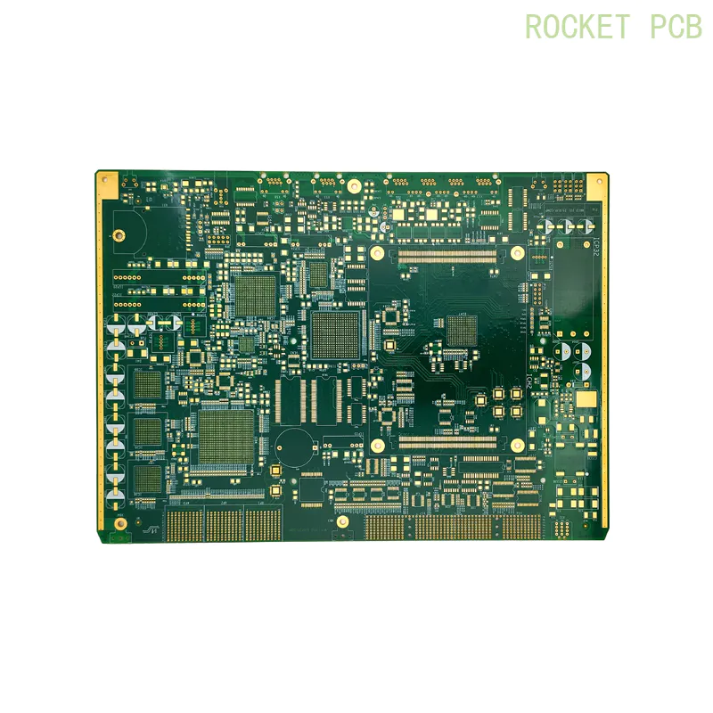
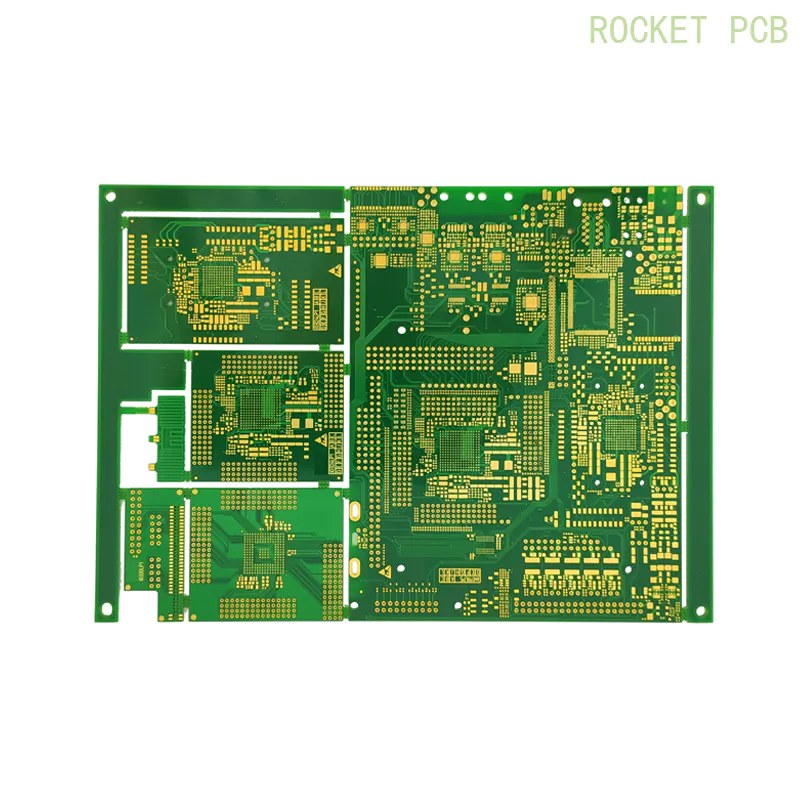
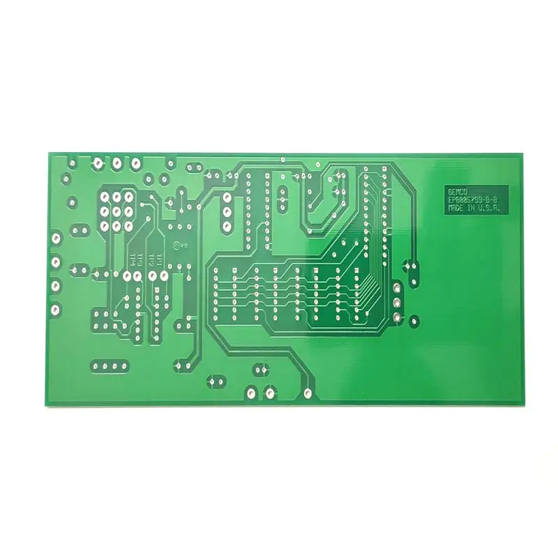
The circuit of double sided PCB & two layers PCB is in two sides of PCB board, and the circuit of double sided PCB board is connected by via in the middle. Double sided PCB is a very important PCB in the circuit boards, which is classified according to the number of layers. There are 4-layer boards, multi-layer boards, high-level multi-layer boards and so on. Of course, if classified according to the PCB application, PCB copper thickness and structure, it also includes double-sided antenna PCB, double-sided metal-base PCB (aluminum substrate / copper substrate / ceramic substrate), high TG double-sided board, thick copper PCB, high-frequency material double-sided PCB, double-sided flexible PCB board, etc.
Double-sided PCB from Rocket is very common in both PCB production and PCB prototype circuits allowing a higher density between components and it makes the layering of tracks an easier process. Compared to the multilayer PCB, double layer PCB do not need laminating but need plating in order to realize the function of vias.
It is widely used in high-tech industries, such as telecommunications, power supply, computer, industrial control, digital products, scientific and educational instruments, medical devices, automobiles, aerospace defense, etc.

1, Cutting Material: Cut out easy-to-process dimensions from the whole sheet of copper clad laminate (CCL).
2, Drilling: Drilling a conductive hole or plug-in hole on the board according to the computer drilling program.
3,
PTH: A thin layer of chemical copper is deposited in the drilled hole,
with the aim of sinking a layer of copper through chemical methods in
non-conductive epoxy glass cloth substrates (or other substrates),
making it easy for the rear plating guide to form the circuit pattern;
4,
Full Plate Copper Plating: The main purpose is to protect the thin
layer of chemical copper from oxidation in the air, forming no copper or
holes in the holes.
5, Circuits (graphics transfer) is pasted with dry film/wet film on board. After exposure and development, circuit graphics are made.
6,
Pattern plating: Wire copper thickening plating on pattern circuit, so
that the hole and pattern copper thickness reached a certain thickness,
can load a certain amount of current
7,
Etching: Fade The graphics ink or dry film, etching off the excess
copper foil to obtain conductive line graphics. Remove the pattern ink
or dry film, etch out the excess copper foil to get the conductive
graphics
8, Remove tin: The tin layer on the formed graph is removed to reveal the required pattern
9,
Silk screen soldermask or paste soldermask dry film: Printing a layer
of soldermask ink on the board, or affixed with a layer of soldermask
dry film, after exposure, development to form soldermask layer, the main
purpose is to prevent short circuit between the lines at the time of
soldering
10, Immersion Gold/HASL:
Immersion gold or spray a layer of tin on the board where it needs to be
welded, making it easy to solder, while also preventing oxidation of
the copper surface at the place
11, Silkscreen: printing some iconic words on the board, mainly convenient for customers to install components
12, Routing: Process the profile of the Board
13, Electrical test: Detecting whether there is an open short circuit in the PCB by means of a closed loop
Detailed PCB manufacturing flow please see from here https://www.rocket-pcb.com/pcb-manufacturing-process-introduction
Rocket PCB has wealthy market practical experience within the area of prototype and midium batch PCB fabrication. Just after decades of industry enhancement and client accumulation, it's founded a great cooperative partnership with world-famous enterprises, and it has been acknowledged by clients when it comes to products top quality stability, technological stage and specialized services, and fashioned a higher brand name recognition in the marketplace.
At Rocket PCB, we have been using top-grade materials,like brand Shengyi, Kingboard material, never cut corners, quality is first-class, our strategy is tiny profits but fast turnover, therefore within the premise of quality assurance, our PCB price is extremely competitive, you're welcome to get quick quotation from here!
Rocket PCB not only supports the production of ordinary double-sided PCB, we are equipped with top-level automation equipment, such as LDI exposure machine, full-automatic exposure machine, vacuum laminating machine, VCP electroplating line, character printing, automatic stacking board machine, etc., so as to improve the processing efficiency and reduce the labor cost. Our production level is more reflected in high-frequency PCB, thick copper PCB, rigid PCB, rigid flex PCB, flexible PCB, RF, metal core, ceramic, Large size board and other advanced PCB technology.
Understand our advanced PCB processing capabilities( Details click here https://www.rocket-pcb.com/capabilities)
1. We provide 24-hour real-time and in-depth technical support to shift your PCB products from conceptual design to mass production. Tailor-made application solutions, like high speed, high capacity and high frequency, press-fit, heat-sink solutions. In general, customers provide gerber files and Rocket senior R&D engineers team audit and optimize them free of charge (Free DRC and DFM)---Our Free DFM and PCB prototype service is the perfect way to ensure that there are no errors in design before entering mass production.
2. For customers with special requirements, we can provide personalized solutions, design drawings, develop new products, and provide relevant technical support according to their needs and combined with our practical experience.
3. Regular board quotation within 2 hours, timely engineering processing and EQ feedback.
4. There will never be MOQ - unlike most manufacturers which need to inspect customers and have minimum order quantity requirements. In rocket PCB, we support PCB prototype producing of 1-5 PCs, which is free of test fees. Choose to cooperate with us, you will benefit from our cost-effective products.
Multiple production lines meet the requirements of mass production and quick turnover of small batches and various prototype PCBs. The factory invested heavily in importing foreign advanced PCB production equipment, such as Burkle laminator, Mitsubishi laser drill, Hitachi mechanical drill, Japan screen automatic exposure machine, LDI, AOI etc, highly automated production. Highly automated production guarantees production efficiency. (See equipment description for details)
As mentioned above, advanced equipment and process optimization ensure the processing efficiency, and our delivery is leading in the industry . We cooperate with DHL, Fedex, TNT, UPS Express Direct , fully meet the customer's time requirements.
The delivery time of other special processes is based on the production process of the board.
1. Quality standard IPC2 or higher according to customer requirements
2. ISO 9001 quality system, TS16949, UL standard, ROHS standard and SGS lead-free certification and related industry certification.
3. Dozens of tests such as open/short circuit testing, AOI, impedance testing, solderability testing, thermal shock testing, metallographic micro-slicing analysis, halogen-free testing, etc
4. Eight major surface treatment technology
HASL
Lead free HASL
Immersion Gold
Immersion Silver
Immersion Tin
OSP
Selective Gold Plating
Hard and Soft Gold
and high-quality ink printing, beautiful and reliable.
Product Message
QUICK LINKS
CONTACT US
Office: (+86) 755 23040566
Tel: (+86) 158 9965 5195
E-mail: sales@rocket-pcb.com
Skype: Hans@Rocket-PCB
Whatsapp: 86 1589965 5195
Office Address: 301 Building/B, Huafeng Digital Technology Industrial Park, Chaoyang Ro, Yanchuan, Songgang,518105 Shenzhen, China.
Plant ADD.: No 69, Lianfeng North Road, Xianxi Area, ChangAn Town, Dongguan, China.