


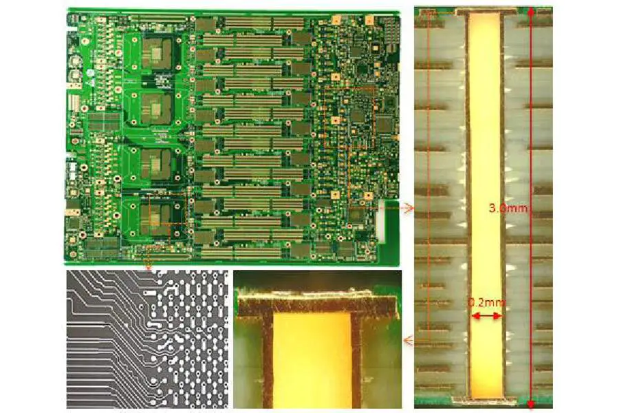
Item | Typical Design |
Layers | 20L |
Size | 18”X24” |
Total Thickness | 0.118” |
DHS | 10mil |
Resin plug A/R | 12: 1 |
L/S | 4.0mil/4.0mil |
Base Material | IS415 |
Surface treatment | OSP |
Soldering condition | Lead Free Reflow (260℃ peak) ×5 Cycle Thermal Stress: 288℃, 10s ×3 Cycle |
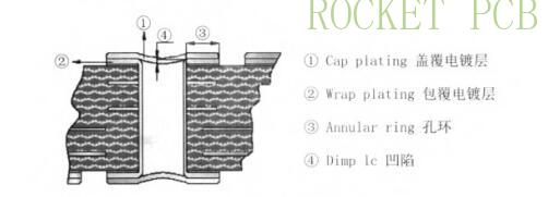
As the speed signal, performance requirements, and routing density increasing, the use of advanced technology of PCB is becoming more and more important, as a result, many BGA placeholder area within the PCB design is adopted the via-in-pad plated over (VIPPO) structure or called plated over filled via (POFV) structure. This VIPPO structure is better than the more traditional type of dog bone pad structure, make the routing between layer and layer space wider, shortening the signal path length, reduce the capacitance, and inductance of these two parasitic effects, thus the high-speed performance is improved.
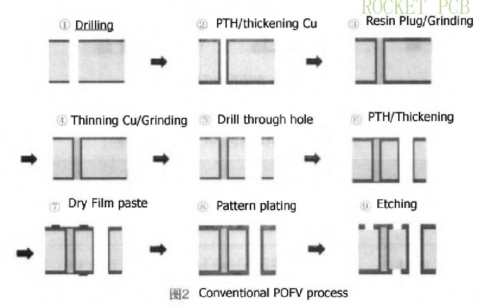
VIPPO/POFV is a method that resin plug vias first and then copper plating over (cladded). Conventional technology is to separate POFV holes from non-POFV holes. Therefore, two electroplating processes are needed to ensure hole wall copper and cap&wrap plating copper thickness. In addition, in order to reduce copper thickness on the face, a thinning copper process is added after the plug holes. At the same time, in order to ensure the thickness of the cap plated copper, the reduced amount of copper can not be too large. Therefore, use the VIPPO process, often appear surface copper thickness exceeds the standard, copper thickness varies greatly, the outer etching difficult and cap copper thin and other problems, and the process is complicated, which adds difficulty to the field operation.
After many tests, data analysis, and defect analysis, different schemes for different quality defects have been formulated to verify, the research summarizes the improvement methods of each process, and obtains remarkable achievements.
Rocket PCB is good at making POFV backplane PCB and POFV BGA board, for more POFV information, please contact Rocket PCB
Fast Quote Now
ADD: No 69, Lianfeng North Road, Xianxi Area, ChangAn Town, Dongguan, China
Technical analysis of VIPPO PCB/ POFV PCB
Do you know what is the key point of resin plug hole used in PCB making?


