


Item | Typical Design |
Layers | 26 |
Size | 20”×16.2” |
Total Thickness | 0.126” |
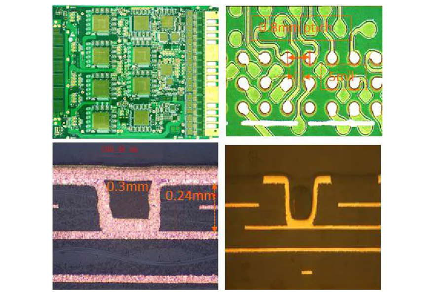
DHS of microvia | 12mil |
A/R of skip microvia | 0.8:1 |
Base copper of microvia | 1Oz |
Registration of microvia | 4mil |
Plated copper thk. | Microvia≥13μm; PTH avg. 25μm, min. 20μm |
Base material | TU872SLK |
The need for PCB boards with higher component density forces PCB designers to use many creative layout techniques in multilayer boards. Skip microvias, dog bone traces, via on pad, microvias and back drilling are all used by designers to increase trace density while maintaining signal integrity requirements.
Via holes are critical for creating high density interconnect (HDI) on a PCB. Via holes are similar to blind vias because they allow the connection between the top or bottom PCB material layer and the inner layer, the blind hole is connected to the next PCB layer, while the skip microvias can be connected to multiple layers.
Skip via PCB also has embedded type (called core via) , which means that the via can connect multiple internal layers in the PCB design. These holes need to be filled with conductive or non-conductive filler. Since electrical conductors are good heat conductors, the density of the device operating at a high current will generate significant heat, and vias with conductive filler may help to dissipate heat from some components.
The aspect ratio of any via will determine how easy it is to electroplate during manufacturing. Skip vias on multilayer PCB may have higher aspect ratio, length-to-width ratio, and they require electroplating solutions with higher surface tension and lower viscosity.
Placing the skip microvia on a printed circuit board requires the same tight tolerance as the through hole. The skip microvia is usually drilled by laser. Slight lateral displacement during the drilling process can deform the inside of the through hole, causing coating problems, the laser drilling process is complicated and, of course, the manufacturing price goes up.
Correct plating will produce a through-hole with a deep continuous conductive layer, which is more durable than other through-holes because the deep plating on the skipping microvia improves its adhesion to the substrate material.
A design technique called via-in-pad plated over (VIPPO) can be used in conjunction with traditional designs to reduce inductance and provide a fast path to direct grounding, which is useful in high frequency circuits where via-in-pad designs (VIPPO) and deep skip microvia can be used to improve the bonding of the pad to the circuit board.
Skip mircrovia should be filled with conductive or non conductive epoxy resin choice epoxy, the first thing to consider is to match the thermal expansion coefficient of the filler with that of the surrounding laminate, the thermal expansion coefficient of non-conductive epoxy resin is close to that of most laminated materials. For this reason, non-conductive epoxy fillers have become very popular and these epoxy resins are also a cheaper option.
Excellent PCB manufacturers such as Rocket PCB have unique advantages in skip microvia HDI field to help you easily solve the problems in PCB manufacturing, is one of the few powerful manufacturers can make high-level HDI boards. If you want to know how Rocket PCB can help you build your next high-speed device, please contact us immediately.


