


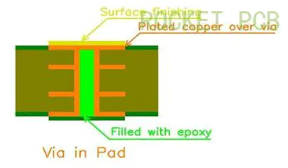
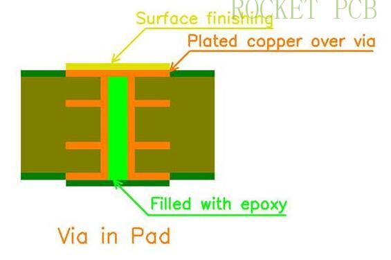
In PCB design, via-in-pad plated over (VIPPO) technology, also called plated over for via (POFV) is widely used in small PCB with limited BGA space. Vias in the pad process allow vias to be plated and hidden under the BGA pad. It requires PCB manufacturers to fill the through holes with epoxy resin, and then copper plating on it to make it almost invisible.
The advantages of vippo technology include:
The holes in the pad can improve the tracking route.
The holes in the pad help to dissipate heat.
The holes in the pad can help reduce the inductance of the high frequency PCB board.
The hole in the pad provides a flat surface for the assembly.
However, there are some disadvantages:
The price of complex manufacturing process is higher than that of common PCB.
If the quality is low, BGA pad may fall off.
Technical principle of via-in-pad hole
Plug the holes in the inner layer with resin and press them together. This technology balances the contradiction between the thickness control of bonding dielectric layer and the design of inner hole filling.
If the inner hole is not filled with resin, when the thermal shock occurs, the board will burst and the scrape board will be directly discarded;
If the resin is not used for plugging, multiple PP sheets need to be pressed to meet the demand of adhesive, but in this way, the thickness of interlayer dielectric layer will increase due to the thickness of PP.
Making point of via-in-pad hole
In order to meet the design requirements of thin dielectric layer, the resin plug hole in the via-in-pad is widely used in high density hdi pcb products.
For the design of the inner buried hole and the blind hole, due to the thinner intermediate design, the inner resin filling process is often needed.
Some products cannot be filled with PP because the size of blind hole is greater than 0.5mm, and resin is also needed to fill the via hole to avoid blind holes without copper.
Production process
Lamination cutting – > Drilling – > PTH - > Plating – > Resin plug hole – > Polishing – > PTH drilling > PTH - > Plating – > Outer dry film – > Graphic plating – > Etching – > S / M coating – > Surface Treatment - >Silkscreen – > Testing – > Packaging & Transportation
Prevention and improvement of the via-in-pad hole
Use appropriate resin ink, control the storage conditions and shelf life of ink.
Standard inspection procedures to avoid empty holes in pad holes. Even with good technology and good conditions to improve the blockage passing rate, the chance of 1 / 10000 may lead to waste, sometimes only because of the gap. This can only be done and repaired by checking the location of the cavity. Of course, the problem of checking resin hole blockage has been discussed, but there seems to be no good equipment to solve this problem.
Choosing the right resin, especially the choice of TG and expansion coefficient, the right production process and the right removal parameters can avoid the problem of separation between the pad and resin after heating.
For the delamination between resin and copper, we found that the thickness of copper on the surface of the hole is more than 15um, and the delamination between resin and copper can be greatly improved.


