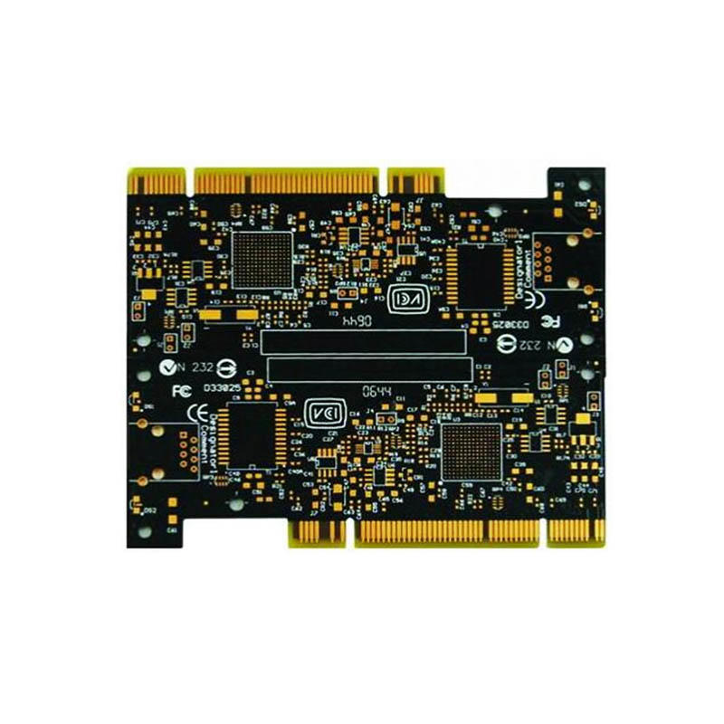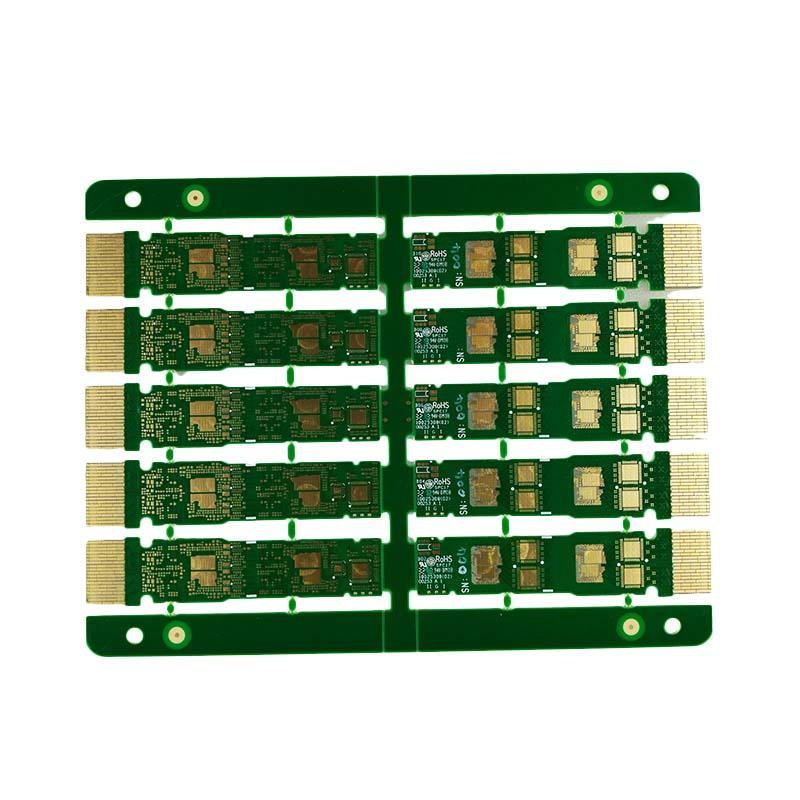
A unique PCBA needs to be interconnected with the motherboard, but it also needs to be easily replaced. Design a gold finger connected to socket, similar to the relationship between the power plug and socket.Because gold has good conductivity, inertia is strong, it can ensure the conductive effect while not oxidizing, at the same time, it can also ensure good enough conductivity after frequent insertion because gold is wear-resistant.
Generally speaking, the golden finger means that these fingers are plated with 5-30u”hard gold. Hard gold has better wear resistance, and can be guaranteed 20,000 times insertion without affecting the quality, it must be more than 5u”thick. However, the processing technology of hard gold is relatively complex, and the high thickness of gold consumes more gold salt, which directly results in high cost. In fact, many PCBs do not need frequent insertion, do not need to do thick gold, or even do not do hard gold, directly do immersion gold replacement (soft gold, gold thickness is generally 1-3 u”). It can effectively reduce the purchase price of PCB.


Standard hard gold finger adopts electroplating, which requires all fingers to conduct electricity during electroplating. Therefore, guide wire will be added below the gold finger. First, a layer of dielectric nickel is plated on the copper surface, and then gold is plated on the nickel layer according to the required thickness.
Before finger gold plating, cover all other non-gold-plated pads with tape, tear off the tape after gold plating, then cover the golden finger with tape. The other pads are made immersion tin, OSP, ENIG and other treatments as required. After the pad treatment is completed, tear off the tape on the golden finger.
1. Firstly, ensure that the length, width, position of the golden finger correspond to the slot, and ensure correct interconnection.
2. Anti-dull KEY SLOT designed on PCB board. Width, height, position and bump in slot match perfectly.
3. Some PCBs need to be designed with shorter fingers. If guide wire cannot be added directly under the fingers, how to conduct electricity in gold plating should be considered.
4. The chamfering angle and depth of the golden finger should be controlled, do not cause the finger short or the remaining thickness too thin after chamfering, result in the board cannot be used.


Copyright © 2026 Rocket PCB Solution Ltd. | All Rights Reserved Sitemap Friendship link: CNC machining heat sink