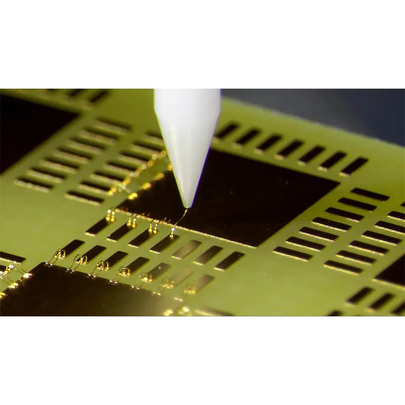
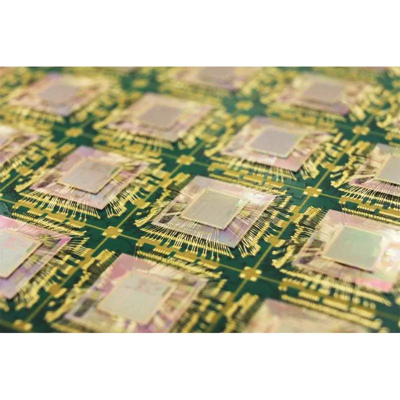
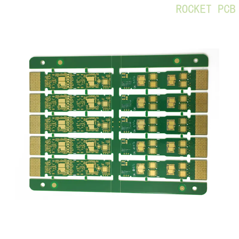
Latest products
material sciences innovation brings us closer to ‘anywhere computing’
by:Rocket PCB
2019-11-17
When Gary Barton pulled a thin, round wafer
Like the sheets in his coat pocket, he didn\'t try to hide his excitement. “It’s cutting-Edge innovation!
The head of IBM\'s global R & D business said he showed a thin-looking piece of metal.
Then, with childlike excitement, he folded the round sheet into a neat triangle, then unfolded it and rolled it into a thin cigarette.
The metal film Dr. Patton is gung-
Ho about represents a major breakthrough in material science that will drive high
Taking performance computing to a new level has pioneered a new paradigm for Silicon and electronic circuits.
Looking closely at the circular patch, you can find that there is a complex circuit network under the shiny surface that looks much like your normal printed circuit board.
The chips are made of silicon and have a future, he said.
At present, these circuits, also known as flexible circuits, are a huge step in portable computing, but the possibilities are endless.
They can power your mobile device, you can embed electronic devices in your body, such as monitoring health parameters, and even active biomedical intervention
Barton told Hindus on the sidelines of the Indian electronics and semiconductors Association (IESA)
Held a summit here last month.
This will allow products to enter the era of \"computing anywhere\", he said, and we have only read about these things in futurist literature or scifi.
What is going on with this flexible wafer?
Silicon wafers are usually hard and thick structures that are added to large wafers to make integrated circuits and other micro-devices.
Research Center at IBM
Barton explained that scientists have selectively cut the silicon substrate into \"very, very thin layers, thinner than paper \".
\"When we do this, we find that there is no significant change in the properties of the material.
This is indeed a major breakthrough.
It\'s sci stuff-fi,” he gushes.
The study, he said, shows that the wafer can be manufactured at room temperature in a conventional process, and that the process is fully scalable.
But how long does it take for something like this to form a product? “Not too long.
It was one of the key breakthroughs IBM showed at the public platform technology forum earlier this year.
Other excitation systems on the insulator (SOI)
The research presented includes breakthroughs in the field of carbon nanotubes and silicon nano-Optoelectronic. Dr.
Barton said that the semiconductor industry is at an important turning point \", when the process engineering has reached the limit to design the material by introducing strain or using a high K metal gate to change the basic properties of silicon to change the properties of the gate oxide;
So far, all the technical processes used to drive the growth of computing power. Currently, Dr.
Barton said that the semiconductor industry is in what he called the 3D era, which is called Fin-
Fets is in 3D integration.
\"This will lead to the real outbreak of mobile Internet devices in the next ten years.
This will get us into 2020, but at some point the 3D will run and we will reach the atomic size limit.
By then, we will enter new materials, and that is where we will enter the era of nanotechnology. Silicon nano wires, and even photon technologies where light replaces conventional electrical signals.
These will be of great benefit to improving the speed of the circuit.
\"But what is driving a surge in demand for computing power,\" asked the doctor.
Barton spoke at the IESA summit.
At the end of the day, this is a \"simple economic problem,\" he said \".
\"You can do smaller features, you can get better performance, you can do more applications, and each feature has a better cost,\" he explained . \".
What you can do on the phone has grown dramatically over the past few years, and guess what, our market has exploded.
\"Consider the difference in transistor prices.
In the past 30 years, the relative price of transistors has dropped by five orders of magnitude, while in the same period, the number of transistors consumed each year has increased by six orders of magnitude.
At the end of the day, it\'s all about the economy.
For example, he compared IBM\'s System 360 with IBM\'s Watson.
The performance of \"dangerous reputation\" artificial intelligence computer system.
A major breakthrough at the time, the core of IBM 360 was a module with six transistors and four resistors and only 10 devices. Patton.
Today, Watson has 360 power chips, one for each.
2 billion transistors, so there is a lot of integration.
But he pointed out that this progress is not limited to highend computing.
This led to a huge explosion in consumer equipment.
From smartphones, games to digital TV, and, of course, the Internet behind all this.
\"Today, there are trillions of devices connected to the internet in some way, and the amount of data has doubled in the past three years. ”Dr.
Cooperation is the key, Barton said.
For example, Samsung\'s range of phones and tablets competes with the iphone and ipad.
Low use of these products
Power version of IBM 32 nm technology for high
Terminal server and network.
\"This optimization is done by working closely with Samsung\'s product team and ARM to figure out how to optimize the entire stack and provide the best service for mobile space.
As you can see, this is rewarding.
\"On the public platform Technology Forum (
Cooperation platform for IBM, Samsung Electronics and global foundry)
More than 75 products of high K metal doors are our products.
But none of this was developed by ourselves.
We work with product companies and partners
Develop technologies that provide the best products.
This is a key theme: collaboration between the product design team and the technical team to deliver the best solution.
\"Today, the whole industry is engaged in large-scale cooperation.
It\'s not that early, but now the regime has changed.
Barton explained.
Given the big challenges ahead, the company has no choice but to continue to innovate, but he stressed that these breakthroughs will not happen on isolated islands.
Custom message