Latest products
intro to printed circuit boards
by:Rocket PCB
2019-10-07
In this Instructure, I will discuss what the printed circuit boards are, where they are used, and the basics of how to make the boards myself.
So sit back and fasten your seat belt and enjoy learning this very important and fun way of making electronics!
Note: This is a guide to getting started.
I\'m sure I don\'t cover a lot, and if you find what you think I should mention in this guide, make sure to mention it in the comments below!
When creating a circuit, it is often necessary to connect multiple electronic components together to perform some useful functions.
There are many different ways to do this: Finally, the board!
Printed circuit board (
Or PCB)
Is a different way of connecting electrical components together.
It is made by a non
It is usually a conductive material of fiberglass.
However, there is one or more layers of copper on the board that can connect the assembly when the copper is etched into the correct pattern.
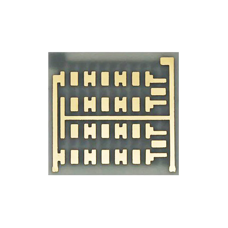
The circuit board in the picture above is made with a CNC machine that mechanically removes the copper layer in a specific place to allow the assembly to be welded on or through the circuit board, and connect together in the right way.
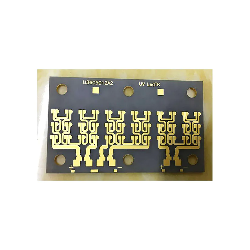
Although this one is not available, many people are covered with welding masks of some color, usually green (but not always)
This helps to stick the solder to the right place.
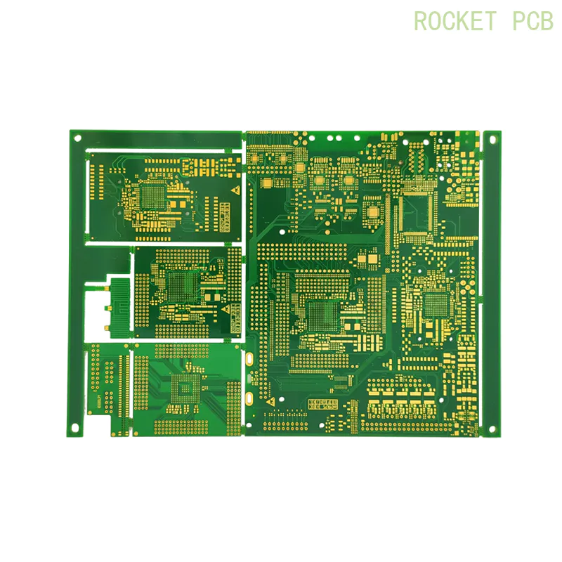
Pcb is perfect for making circuits because they are: pcb is included in almost all electronic products;
Computers, mice, electric scooters, refrigerators, screens, mobile phones and countless other devices.
World market for printed circuit boards (PCBs)
An estimated $60.
The value reached 2 billion in 2014 and will only get bigger and bigger: the first step in designing a PCB is to know what you want to do.
There may be a lot of PCB design, it may be very simple;
It depends entirely on what circuit you are doing.
But no matter what you end up doing, it\'s helpful to have a program to organize all of this for you and give you the tools you need to open the schematic (
Abstract drawings of all parts and connections you need)
To the final layout of the board.
From there you can export your file and send it out for forgery.
Some programs for PCB design: all of them are designed to do the same thing;
Help you make your PCB.
You need to create something: a board shape to define the size and shape your board is placed by the Assembly: where is your part?
Tracking routes: These connect all your component files export: export the manufacturer\'s industry standard gerber file. Your circuit board can also have a lot of other circuit components, and I\'ll briefly list some of them here in order to inspire your imagination: So you want to make a PCB?
Well, there are many different ways you can use.
The most efficient and easy way for Fab house is to send your gerber file to fab house.
These files were created by you in the circuit creation program and made a circuit board for you.
I will discuss these in more detail in the next steps.
CNC machine if you have access to the motherboard, you can also create the motherboard using the CNC machine.
I personally used LPKF made machine at work, it is specially designed for other machine companies to make circuit boards and other factories
Another factory is specially designed for hobby, can carve 3d shape into soft material block, can also double
Double-sided copper clad board for PCB manufacturing.
Finally, the cheapest of the three;
Etching your own board at home with multiple stages of chemicals to eat the area between the marks.
I will let the audience know how this interesting process works: the popular option to get PCBs is made by a fab house.
These are professional facilities that handle the construction of possibly thousands of planks per day.
The quality of each fab house is different and the tolerances for tracking width, hole size and other specificity are also different, such as cutting slots, so you should do the research before sending the file anywhere.
Shipping will be discounted in some places, but the lead time will be longer, or only small batches will be offered, so it\'s good for the prototype, but not when you need a lot of boards.
Everyone has a place they like and you can choose which one to use.
Here are a few: PCB shoppers can allow you to compare multiple different fab houses and identify places that fit your needs.
More information: Old article)
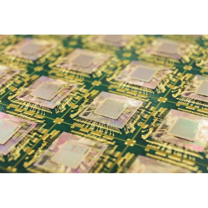
Picture: you have bare PCB and the next step is to add your component.
These need to be welded, but there are many more ways to do everything in addition to doing it manually.
I said there are other ways, but as long as you don\'t have a huge assembly and a stable soldering iron, as long as you don\'t have dozens or hundreds of plates to weld, it\'s still a good way to place the assembly manually.
Take the tweezers out!
Pick and place machines automatically grab components and place them in the right place on the board.
These machines are so cool!
You should look up their videos in use, which will save you a lot of time assembling electrical components.
But these are expensive!
If your fab house is adding components, they may provide placement, in which case they may use this machine for a large number of the same boards.
The return oven can be used with pick-up and placement machines or hand placement, but is usually used for surface mounting parts.
Apply tin paste before the element is placed.
Then, put the PCB into the oven, the temperature rises, and then drops again at an exact interval.
This is hot enough to melt and reflow paste and fix all the components on the pad but not too hot to damage any assembly.
As surface mounting components are becoming more and more popular, wave soldering has been replaced by a reflow oven, but is still an effective method.
The heated solder is pumped with a waveform, and the plate enters the wave to quickly weld multiple components to the PCB.
There are some different, very cool PCBs.
Flexibility: these plates can be bent and twisted.
While not much to use, they can be useful when devices need to be small and lightweight, for example in wearable devices. 3d-printed (Voxel8)
: At least one company is now making a 3d printer that can integrate conductive traces with printed plastic layers.
In this way, electronic devices can be integrated with mechanical components;
Three dimensions.
These technologies are not very popular at the moment, but may be used more and more if prices fall.
Make sure to focus on future flexible 3d printing products!
Thank you for reading my instructions and I hope you have a new understanding of the pcb!
So sit back and fasten your seat belt and enjoy learning this very important and fun way of making electronics!
Note: This is a guide to getting started.
I\'m sure I don\'t cover a lot, and if you find what you think I should mention in this guide, make sure to mention it in the comments below!
When creating a circuit, it is often necessary to connect multiple electronic components together to perform some useful functions.
There are many different ways to do this: Finally, the board!
Printed circuit board (
Or PCB)
Is a different way of connecting electrical components together.
It is made by a non
It is usually a conductive material of fiberglass.
However, there is one or more layers of copper on the board that can connect the assembly when the copper is etched into the correct pattern.
The circuit board in the picture above is made with a CNC machine that mechanically removes the copper layer in a specific place to allow the assembly to be welded on or through the circuit board, and connect together in the right way.
Although this one is not available, many people are covered with welding masks of some color, usually green (but not always)
This helps to stick the solder to the right place.
Pcb is perfect for making circuits because they are: pcb is included in almost all electronic products;
Computers, mice, electric scooters, refrigerators, screens, mobile phones and countless other devices.
World market for printed circuit boards (PCBs)
An estimated $60.
The value reached 2 billion in 2014 and will only get bigger and bigger: the first step in designing a PCB is to know what you want to do.
There may be a lot of PCB design, it may be very simple;
It depends entirely on what circuit you are doing.
But no matter what you end up doing, it\'s helpful to have a program to organize all of this for you and give you the tools you need to open the schematic (
Abstract drawings of all parts and connections you need)
To the final layout of the board.
From there you can export your file and send it out for forgery.
Some programs for PCB design: all of them are designed to do the same thing;
Help you make your PCB.
You need to create something: a board shape to define the size and shape your board is placed by the Assembly: where is your part?
Tracking routes: These connect all your component files export: export the manufacturer\'s industry standard gerber file. Your circuit board can also have a lot of other circuit components, and I\'ll briefly list some of them here in order to inspire your imagination: So you want to make a PCB?
Well, there are many different ways you can use.
The most efficient and easy way for Fab house is to send your gerber file to fab house.
These files were created by you in the circuit creation program and made a circuit board for you.
I will discuss these in more detail in the next steps.
CNC machine if you have access to the motherboard, you can also create the motherboard using the CNC machine.
I personally used LPKF made machine at work, it is specially designed for other machine companies to make circuit boards and other factories
Another factory is specially designed for hobby, can carve 3d shape into soft material block, can also double
Double-sided copper clad board for PCB manufacturing.
Finally, the cheapest of the three;
Etching your own board at home with multiple stages of chemicals to eat the area between the marks.
I will let the audience know how this interesting process works: the popular option to get PCBs is made by a fab house.
These are professional facilities that handle the construction of possibly thousands of planks per day.
The quality of each fab house is different and the tolerances for tracking width, hole size and other specificity are also different, such as cutting slots, so you should do the research before sending the file anywhere.
Shipping will be discounted in some places, but the lead time will be longer, or only small batches will be offered, so it\'s good for the prototype, but not when you need a lot of boards.
Everyone has a place they like and you can choose which one to use.
Here are a few: PCB shoppers can allow you to compare multiple different fab houses and identify places that fit your needs.
More information: Old article)
Picture: you have bare PCB and the next step is to add your component.
These need to be welded, but there are many more ways to do everything in addition to doing it manually.
I said there are other ways, but as long as you don\'t have a huge assembly and a stable soldering iron, as long as you don\'t have dozens or hundreds of plates to weld, it\'s still a good way to place the assembly manually.
Take the tweezers out!
Pick and place machines automatically grab components and place them in the right place on the board.
These machines are so cool!
You should look up their videos in use, which will save you a lot of time assembling electrical components.
But these are expensive!
If your fab house is adding components, they may provide placement, in which case they may use this machine for a large number of the same boards.
The return oven can be used with pick-up and placement machines or hand placement, but is usually used for surface mounting parts.
Apply tin paste before the element is placed.
Then, put the PCB into the oven, the temperature rises, and then drops again at an exact interval.
This is hot enough to melt and reflow paste and fix all the components on the pad but not too hot to damage any assembly.
As surface mounting components are becoming more and more popular, wave soldering has been replaced by a reflow oven, but is still an effective method.
The heated solder is pumped with a waveform, and the plate enters the wave to quickly weld multiple components to the PCB.
There are some different, very cool PCBs.
Flexibility: these plates can be bent and twisted.
While not much to use, they can be useful when devices need to be small and lightweight, for example in wearable devices. 3d-printed (Voxel8)
: At least one company is now making a 3d printer that can integrate conductive traces with printed plastic layers.
In this way, electronic devices can be integrated with mechanical components;
Three dimensions.
These technologies are not very popular at the moment, but may be used more and more if prices fall.
Make sure to focus on future flexible 3d printing products!
Thank you for reading my instructions and I hope you have a new understanding of the pcb!
Custom message