What is the PCB
by:Rocket PCB
2020-07-29
In the electronics industry (one of the key components are referred to as the PCB
PrintedCircuitBoard)
, Chinese name called printed circuit board)
。
This is a basic component, resulting in a lot of people are hard to explain what is PCB.
This article will explain in detail the composition of PCB, and some of the terms commonly used in PCB field.
In the next few pages, we will discuss PCB proofing, the components of the circuit board factory, circuit board factory, including some of the terminology, brief assembly method, as well as the introduction of the PCB design process.
Circuit board PCB/PCB/PCB (
PrintedCircuitBoard)
Is one of the most common way, also can be called 'printedwiringboards' or 'printedwiringcards'.
Before there were PCB circuit through the point-to-point connection.
The reliability of this method is very low, because with the aging of the circuit, circuit breakdown can lead to circuit nodes open circuit or short circuit.
When the development of electronic industry from the vacuum tube, relay silicon semiconductor and integrated circuit, the size of the electronic components is reduced, prices are falling.
The emergence of electronic products is more and more frequently in the field of consumption, encourage manufacturers to look for a smaller and more cost-effective solutions.
So the PCB was born.
PCB looks like a multi-layer cake or lasagna & # 8211;
Made of different material layers, through heat and adhesive pressed together.
Start with the middle tier FR4 glass fiber board.
PCB substrate are generally glass fiber.
In most cases, the PCB of the glass fiber base material is generally referred to as 'FR4' this kind of material.
'FR4' this solid material is glass fiber board, it gave the hardness and thickness of the PCB.
Besides FR4 glass fiber board this base material, high temperature and flexible plastic (
Polyimide or similar)
On the production of flexible circuit boards, etc.
You may find that there are different thickness of the PCB;
Dongguan Rocket PCB circuit of the thickness of the product, however, most of them are 1.
6mm。
There are some other electronics industry products also used the other thickness, this is all according to the customer's product requirements to arrange production.
Cheap PCB hole hole plate and the hole hole plate (
Pictured above)
Is made of epoxy resin or phenol materials, lack of FR4 glass fiber board the durability, but much cheaper.
When in the circuit board welding things, will smell a lot of peculiar smell.
This type of base material, is often used in very low-end consumer goods.
Phenolics has lower thermal decomposition temperature, carbide welding time is too long can lead to its decomposition, and send out an unpleasant taste.
The introduction is a very thin layer of copper foil, in the production of adhesives by heat and suppress them above the base material.
In double-sided circuit boards, copper foil to suppress the pros and cons of base material.
In some low cost, may suppress copper foil on one side of the base material.
When we refer to 'double panel' or 'two layer board', refers to our lasagna with two layers of copper foil.
Different PCB circuit board design, of course, the amount of copper foil layer may be so little 1 layer, or more than 16 layer.
PCB circuit boards are many copper layer thickness, but also made the unit weight, generally USES the weight of the copper uniform coverage of a square foot (
Ounce of oz)
To represent.
Most of the copper thickness is 1 oz (PCB
1oz=35um)
, but there are some high power PCB circuit boards may be used 2 oz or 3 oz copper thickness.
Will an ounce (
盎司)
Conversion, per square foot is about 35 um or 1.
4 mil thick copper.
阻焊层(
Resistance welding)
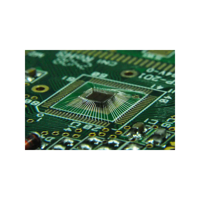
The above is the resistance welding layer on copper layer.
This layer to make PCB circuit boards look is green.
Resistance welding layer covering above the layer of copper wire, prevent to go on the PCB line and other metal contact, soldering, or other conductive objects cause a short-circuit.
Resistance welding layer exists, we can be in the right place for welding, and prevent the solder bridge.
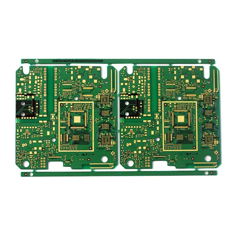
Double spray tin circuit board in the above example, we can see that the resistance welding covers most of the PCB (
Including the line)
, but out of silver grommet and SMD pads, for welding.
In general, resistance welding are green, but almost all of the color can be used for resistance welding.
SparkFun board most is red, but the IOIO board with white, LilyPad board is purple.
In resistance welding layer above, it is white silk screen layer.
On the screen printing layer of PCB proofing with letters, Numbers, and symbols, so that we can convenient to assemble and guide people to better understand the card design.
We often use silk screen layer symbol marking some pin or LED function, etc.
Silk screen layer is one of the most common color is white, also, silk screen layer can make almost any color.
Black, grey, red and even yellow silk screen layer are not uncommon.
However, seldom see a single board has a variety of color screen printing layer.
Rocket PCB Solution Ltd. have now decided to extend our company in other countries.
Crazy about products? Rocket PCB Solution Ltd. is the place you must shop at, do visit Rocket PCB to check out our latest collections!
Regularly improving pcb making service in accordance with customer feedback is a great way to show your brand listens and cares.
Custom message
