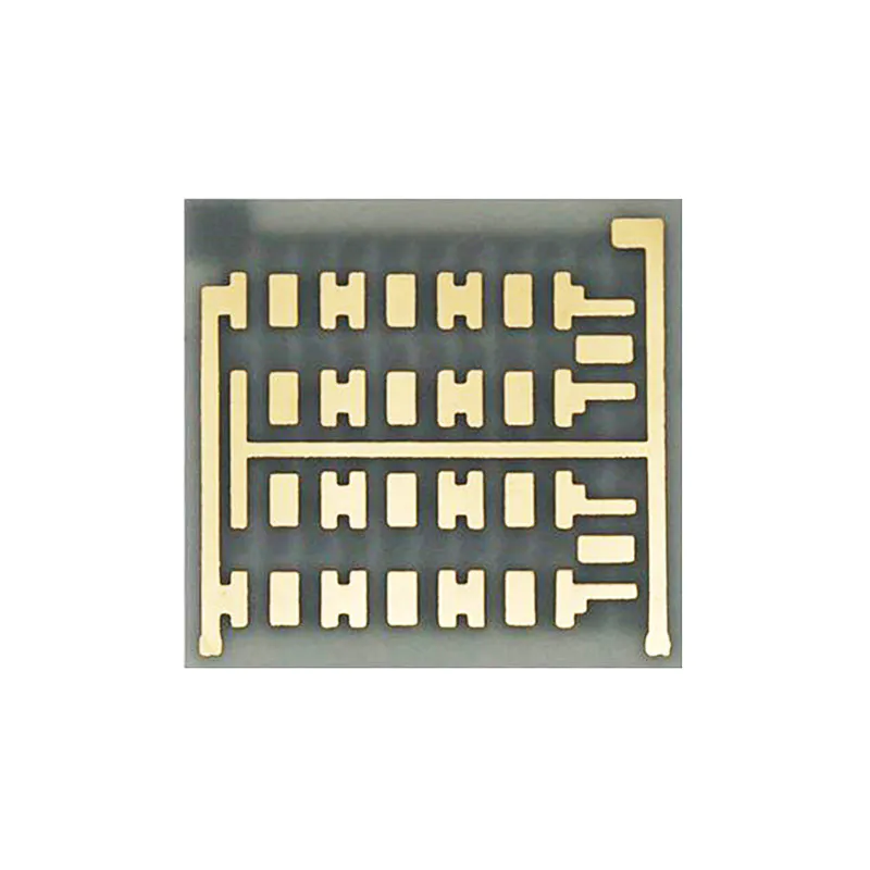
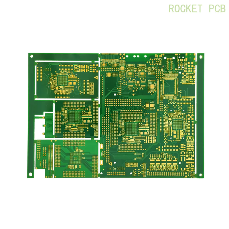
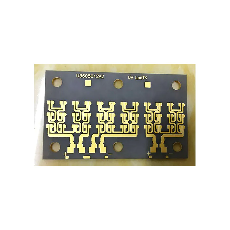
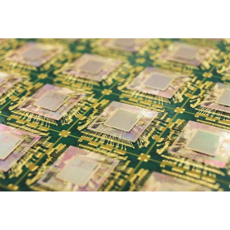
What are the typical features of multilayer circuit board proofing
1, CAM optimization in general, proofing will want to get high quality PCB CAM processing is performed when its production, when doing a CAM processing is first and foremost to appropriate compensation of the line width, spacing and the optimization of welding plate to ensure that do. So only CAM optimization will do a good job, will let the multilayer PCB circuit for better signal, thus ensuring the quality of the multilayer circuit board proofing. 2 proofing, reasonable process of high quality PCB to ensure that the process is reasonable, neat degree of the device can be observed to determine, proofing, after reflow soldering and wave soldering device are all very neat, and tin not good even the phenomenon of welding on 3, clean and tidy appearance after multilayer circuit board pull out of the product first to observe whether smooth appearance, its the edges have burr, PTH holes have holes, also look at the base material of sandwich plate, wire resistance welding between the membrane and the surface have a blister or foam and layered phenomenon, as well as the resistance welding membrane waves, did not appear on the wrinkling, the phenomenon of grain. Impedance circuit board production manufacturers