
English


Item | Typical Design |
Layers | 20L |
Size | 18”X24” |
Total Thickness | 0.118” |
DHS | 10mil |
Resin plug A/R | 12: 1 |
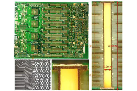
L/S | 4.0mil/4.0mil |
Base Material | IS415 |
Surface treatment | OSP |
Soldering condition | Lead Free Reflow (260℃ peak) ×5 Cycle Thermal Stress: 288℃, 10s ×3 Cycle |
In PCB design, the via-in-pad plated over (VIPPO) technology, also known as plated over for via (POFV) technology, is widely used in small PCBs where BGA space is limited. The over-hole in the padding process allows the over-hole to be plated and hidden under the BGA pad. It requires the PCB manufacturer to fill the through-hole with epoxy resin and then plate copper to make it almost invisible.
Advantages of VIPPO Technology include:
Holes in the pad improve trace routing.
Holes in the pad help dissipate heat.
Holes in the pad help reduce the inductance of high-frequency PCBs.
Holes in the pad provide a flat surface for the assembly.
The technical principle of via-in-pad holes
The holes in the inner layers are plugged with resin and then pressed together. This technique balances the contradiction between the thickness control of the bonding dielectric layer and the design of the inner hole filling.
If the inner holes are not filled with resin, the plate will burst when a thermal shock occurs, and the scraper will be scrapped outright.
If the holes are not plugged with resin, multiple PP sheets need to be pressed to meet the adhesive requirements, but this increases the thickness of the interlayer dielectric layer due to the thickness of the PP.
Critical points of via-in-pad hole fabrication
To meet the design requirements of thin dielectric layers, resin plug holes in solder pads are widely used in high-density HDI PCB products.
For the design of in-pad holes and blind holes, the in-pad resin filling process is often required due to the thin intermediate design.
Some products can not be filled with PP because the blind hole size is more significant than 0.5mm, but they also need to fill the over hole with resin to avoid copper-free blind holes.
Production process
Laminate cutting → drilling → PTH → plating → resin filled hole → polishing → PTH drilling → PTH → plating → outer dry film → graphic plating → etching → S/M coating → surface treatment → screen printing → testing → packaging and transportation
via-in-pad hole prevention and improvement
Use suitable resin ink and control the ink's storage condition and shelf life.
Standard inspection procedures to avoid cavities in pad holes. Even with good technology and conditions to improve the plugging-through rate, the one in ten thousand chance may lead to waste, sometimes just because of the gap. This can only be accomplished and repaired by checking the location of the cavity.
Choosing the suitable resin, especially for TG and expansion coefficient, the proper production process, and removal parameters can avoid the problem of pad and resin separation after heating.
For the delamination of resin from copper, we found that a copper thickness greater than 15um on the hole surface can significantly improve the delamination of resin from copper.
As the speed signal, performance requirements and routing density increasing, the use of advanced technology of PCB is becoming more and more important, as a result, many BGA placeholder area within the PCB design is adopted the via-in-pad plated over (VIPPO) structure or called plated over filled via (POFV) structure. These VIPPO structure is better than the more traditional type of dog bone pad structure, make the routing between layer and layer space wider, to shorten the signal path length, reduce the capacitance and inductance of these two parasitic effects, thus the high speed performance is improved.
VIPPO/POFV is a method that resin plug vias first and then copper plating over (cladded). Conventional technology is to separate POFV holes from non-POFV holes. Therefore, two electroplating processes are needed to ensure hole wall copper and cap&wrap plating copper thickness. In addition, in order to reduce copper thickness on the face, a thinning copper process is added after the plug holes. At the same time, in order to ensure the thickness of the cap plated copper, the reduce amount of copper can not be too large. Therefore, use the VIPPO process, often appear surface copper thickness exceeds the standard, copper thickness varies greatly, the outer etching difficult and cap copper thin and other problems, and the process is complicated, which adds difficulty to the field operation.
After many tests, data analysis and defect analysis, different schemes for different quality defects have been formulated to verify, the research summarizes the improvement methods of each process and obtains remarkable achievements.
For more information, please contact Rocket PCB.
QUICK LINKS
CONTACT US
Office: (+86) 755 23040566
Tel: (+86) 158 9965 5195
E-mail: sales@rocket-pcb.com
Skype: Hans@Rocket-PCB
Whatsapp: 86 1589965 5195
Office Address: 301 Building/B, Huafeng Digital Technology Industrial Park, Chaoyang Ro, Yanchuan, Songgang,518105 Shenzhen, China.
Plant ADD.: No 69, Lianfeng North Road, Xianxi Area, ChangAn Town, Dongguan, China.


Copyright © 2026 Rocket PCB Solution Ltd. | All Rights Reserved Sitemap Friendship link: CNC machining heat sink

