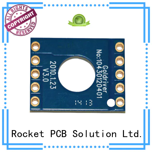


Making process control of thick copper board
Drilling aperture
Due to the need to go through two copper plating, the finished product aperture needs to be compensated accordingly
After two times copper plating need to complete the outer layer pattern, soldermask, silkscreen and other processes, so the Pin hole has the corresponding control
1, Design of first registration pin hole 3.175mm, ensure the accuracy of the first outer layer
2, Design second time of pin holes, due to after two copper plating the pin hole diameter is smaller, so the original design need to do the corresponding compensation, this pin hole directly affect two times of the outer layer, soldermask, silkscreen registration accuracy
First time soldermask control
1, Base material position filling ink, guarantee smooth with copper surface
2, Nail bed making, try to print both sides of soldermask at the same time
3, Block Point Network production, requires 36T mesh yarn
4, Printing ink viscosity ≥300dpa.s, ensure that the substrate and copper surface high difference can fill
5, Pre-baked, after printing static 2H or more
6, Contraposition Wash the remaining ink off the line on the development line, line open window unilateral shrinkage 2-3mil to ensure the accuracy of the position
7, After-baking, segmented baking, to ensure that the substrate position of the ink completely cured
Second time copper Plating
Rough treatment of board surface before drilling and plating, drilling electroplating is the same as double board process , copper plating time 20min , turn off the grinding brush after first time copper plating
Second time outer layer pattern
Pre-treatment turn off the grinding brush, only over pickling, to prevent the substrate bit copper skin wrinkle, to prevent the film from wrinkling resulting in second graphics seepage plating.


Copyright © 2026 Rocket PCB Solution Ltd. | All Rights Reserved Sitemap Friendship link: CNC machining heat sink