
English


Typical Index | Design Features |
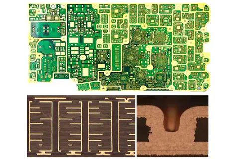
Layers | 24 |
Size | 18.5”× 24.5” |
Total Thickness. | 0.098” |
DHS | PTH 10mil Microvia 3mil |
A/R | PTH 10:1 microvia 0.8:1 |
L/S | 4mil/4mil |
Base Material | M6 |
Soldering condition | Lead Free Reflow (260℃ peak) ×5 times |
What are the advantages of HDI PCBs?
Superior versatility: HDI PCBs are typically used in applications where weight, space, reliability, and performance are significant concerns. As a result, HDI circuit boards are widely used in aerospace, consumer goods, electronics, and computer applications.
Compact design: These high-density boards use blind holes, buried holes, or a combination of both. Sometimes, these boards also integrate microvias with minimal diameters. As a result, more space is needed to accommodate more components.
Higher reliability: Multilayer high-density interconnect boards provide a solid interconnection of stacked through-holes. This makes them highly reliable when used in extreme and adverse environments.
Improved signal transmission: HDI-printed circuit boards use small components. These boards incorporate through-hole and blind-hole technology in the solder pads, resulting in closer proximity between components. This helps to reduce the possibility of signal loss and crossover delays, thereby increasing signal transfer rates. This contributes to the overall performance of high-density interconnect printed circuit boards.
Cost-effective design: High-density boards help reduce product size without compromising product quality. Thus, with HDI technology, an 8-layer through-hole PCB can be reduced to a 4-layer HDI micro-hole PCB, yet the 4-layer HDI PCB has the same or better wiring capability than an 8-layer PCB. High-quality HDI designs can be obtained at a cost-effective price.
The quality of high-order HDI board and copper foil substrate becomes more and more strict with the trend of lightweight, short, high-function,high-density and high reliability of electronic system.
In the manufacture of copper foil substrate, the thickness and quality of copper foil substrate will be affected by the inspection specifications of rawmaterial glass fibre cloth, film baking conditions, glue content, glue flow rate, gelatinization time, conversion degree and storage conditions, etc. The control of thickness and quality needs to review the ownership process and improve the process capability to a certain extent. At present, copper foil base material manufacturers have gradually changed to non-contact laser thickness testing instead of manual centimeter sampling.
Rocket PCB is one of the few local PCB manufacturers that can provide high multilayer PCB board and any-layer interconnection HDI. It has complete quality, advanced technology and process. We focuse on high-level automotive electronics, consumer electronics, focusing on high-end PCB applications, platform advantages are obvious. Considering the process and staged via hole of mass production, the company has 64 layers of high-rise PCB board at present, and the order of HDI increase can reach 5 orders, with the minimum line width and line spacing of 40/45 micron. It can be seen that the company's high-level PCB board and HDI technology are in the leading level in China, and in terms of any layer of interconnected HDI that best reflects the technical capabilities of HDI, the company is also one of the few local manufacturers that can produce any layer of interconnected HDI. Driven by the two trends of electronic products: light, short and high-speed, high-frequency, the industrial structure of PCB has been constantly adjusted to high-end, and the proportion of high-end products represented by FPC, high multilayer pcb board and high-level HDI has been continuously increased.
QUICK LINKS
CONTACT US
Office: (+86) 755 23040566
Tel: (+86) 158 9965 5195
E-mail: sales@rocket-pcb.com
Skype: Hans@Rocket-PCB
Whatsapp: 86 1589965 5195
Office Address: 301 Building/B, Huafeng Digital Technology Industrial Park, Chaoyang Ro, Yanchuan, Songgang,518105 Shenzhen, China.
Plant ADD.: No 69, Lianfeng North Road, Xianxi Area, ChangAn Town, Dongguan, China.


