


Exploring the Interplay between Circuit Board Development, Assembly, and PCB Prototyping
Introduction
Circuit board development, assembly, and PCB prototyping are interconnected processes essential in creating electronic devices. PCB prototyping, in particular, holds significant importance in ensuring the success of circuit board development and assembly projects. In this article, we will explore the role of PCB prototyping and provide valuable insights to address common user questions. Users can make informed decisions and optimize their projects by understanding the significance of PCB prototyping and its synergies with circuit board development and assembly.
Significance of PCB Prototyping
PCB prototyping is a crucial step in circuit board development and assembly. It allows designers to transform their ideas into physical prototypes, visually representing the circuit design before mass production. By creating a prototype, designers can test and validate the functionality and feasibility of their plans, ensuring that they meet the desired specifications and performance requirements. This early-stage evaluation helps identify and rectify any potential design flaws or optimization opportunities, leading to improved performance and reliability in the final product.
The primary aim of this article is to address common user questions and provide professional insights regarding PCB prototyping. We understand that users seeking PCB prototyping services often have concerns and queries about the process, its benefits, suitable techniques, and considerations when choosing a service provider. By offering comprehensive information and expert guidance, we aim to empower users to make informed decisions and navigate the complexities of PCB prototyping effectively.
Throughout the article, we will delve into the benefits of PCB prototyping, discuss different prototyping methods and techniques, highlight considerations when selecting a service provider, and explore troubleshooting strategies. We will also emphasize the iterative nature of PCB prototyping, where multiple iterations and refinements contribute to developing an optimized circuit board design. With this comprehensive understanding, users can harness the full potential of PCB prototyping and achieve successful outcomes in their circuit board development and assembly projects.
II. Understanding PCB Prototyping
A. Definition of PCB Prototyping and Its Role in the Development Process
Before mass production, PCB prototyping refers to creating a functional prototype of a printed circuit board (PCB). It involves designing and fabricating a small-scale version of the PCB to validate the design, test its functionality, and identify any potential issues or improvements.
In the development process of electronic devices, PCB prototyping plays a crucial role. It allows engineers and designers to evaluate the feasibility of their circuit board designs, verify the functionality of the components and connections, and make necessary adjustments or optimizations before moving on to large-scale production. By creating a prototype, designers can physically examine and test their PCB designs, ensuring they meet the desired specifications and performance requirements.
B. Importance of Accurate PCB Prototyping for Successful Circuit Board Assembly
Accurate PCB prototyping is essential for achieving successful circuit board assembly and the overall performance of electronic devices. Here are a few key reasons why accurate prototyping is crucial:
1. Verification of Design: PCB prototyping enables designers to validate their circuit board designs and ensure they work as intended. By physically constructing and testing a prototype, designers can identify design flaws, errors, or potential issues that may arise during the assembly process.
2. Functionality Testing: Prototyping allows engineers to test the PCB and its components' functionality. This includes checking signal integrity, power distribution, voltage levels, and overall circuit performance. Pushing the prototype can identify and rectify any design shortcomings or functional problems before production.
3. Optimization Opportunities: Prototyping provides an opportunity to optimize the design for better performance, cost-effectiveness, and manufacturability. By examining the prototype, engineers can identify areas where improvements can be made, such as component placement, routing, thermal management, and overall design efficiency.
C. Key Factors to Consider When Choosing a PCB Prototyping Service Provider
Several factors should be considered when selecting a PCB prototyping service provider to ensure the best possible outcomes. Here are some key factors to keep in mind:
1. Expertise and Experience: Look for a service provider with a proven track record and experience in PCB prototyping. Evaluate their knowledge in handling various types of designs and their familiarity with industry standards and best practices.
2. Manufacturing Capabilities: Consider the service provider's manufacturing capabilities, including the technologies, equipment, and materials they utilize. Ensure they accommodate your design requirements, such as layer count, board size, and complex features.
3. Quality Standards: Verify the service provider's quality control processes and certifications. They should follow industry standards like IPC (Association Connecting Electronics Industries) and have quality management systems to ensure the production of reliable and high-quality prototypes.
4. Turnaround Time: Assess the service provider's ability to deliver prototypes within your required timeframe. Quick turnaround times are crucial, especially for time-sensitive projects or when iterative prototyping is necessary.
5. Communication and Support: Effective communication is vital during the prototyping process. Ensure the service provider has clear communication channels and is responsive to your inquiries or concerns. Look for providers that offer technical support and guidance throughout the prototyping stage.
By considering these factors, you can select a PCB prototyping service provider that aligns with your project's requirements and facilitates the successful development of your circuit board design.
III. Benefits of PCB Prototyping
A. Ensuring Design Functionality and Feasibility through Prototyping
One of the primary benefits of PCB prototyping is the ability to ensure design functionality and feasibility before mass production. By creating a prototype, designers can validate their design concepts and test the functionality of the PCB. This step allows them to identify any potential issues or challenges that may affect the performance of the circuit board. Through prototyping, designers can make necessary adjustments and refinements to ensure the final design meets the desired functional requirements.
B. Identifying and Resolving Design Flaws or Optimization Opportunities Early On
PCB prototyping enables the early detection and resolution of design flaws or optimization opportunities. By fabricating a prototype and conducting thorough testing, designers can identify any design flaws, errors, or inefficiencies in the circuit board design. They can assess signal integrity, power distribution, thermal management, and overall performance. This early identification of design issues allows for timely corrections and improvements, reducing the risk of costly revisions during mass production.
C. Facilitating Collaboration between Design and Assembly Teams for Seamless Integration
Prototyping also facilitates collaboration between design and assembly teams, leading to the seamless integration of the PCB into the final product. The prototype is a fundamental reference point that helps both teams understand the design intent, component placement, and interconnections. Through effective communication and collaboration, any compatibility issues or manufacturing constraints can be identified and addressed early in the process. This collaboration ensures a smooth transition from the design phase to the assembly phase, minimizing errors and streamlining the production process.
D. Reducing Time-to-Market and Overall Project Costs through Efficient Prototyping Iterations
Efficient prototyping iterations contribute to reduced time-to-market and project costs. Designers can gradually refine and optimize the design by conducting multiple prototype iterations. Each iteration allows them to implement improvements, validate the changes, and verify the desired outcomes. This iterative process helps in reducing the time spent on rework during mass production, as potential issues are addressed and resolved in the prototyping stage. Additionally, identifying and fixing design flaws early on minimizes the overall project costs associated with revisions, rework, and potential product failures.
PCB prototyping offers several significant benefits. It ensures the functionality and feasibility of the design, enables early identification and resolution of design flaws, facilitates collaboration between design and assembly teams, and reduces time-to-market and overall project costs through efficient prototyping iterations. Incorporating PCB prototyping into the development process is a valuable step in ensuring the successful realization of high-quality and reliable circuit board designs.
IV. PCB Prototyping Methods and Techniques
A. Common PCB Prototyping Methods
Several standard methods are used for PCB prototyping, each offering unique advantages and suitability for different design requirements. Here is an overview of some commonly employed techniques:
1. Subtractive Prototyping: This method involves starting with a copper-clad substrate and removing unwanted copper using etching techniques. The desired circuit pattern is created by applying a resist and etching away the excess copper, leaving behind the circuit traces.
2. Additive Prototyping: Compared to subtractive prototyping, additive techniques build up the circuitry layer by layer. This can be achieved through conductive inkjet printing or electroplating, where conductive materials are selectively deposited to form the circuit pattern.
3. Milling: PCB milling involves using a CNC (Computer Numerical Control) machine to mechanically remove unwanted copper from the substrate, creating the desired circuit traces and features. It is suitable for designs that require high precision and complex circuitry.
4. 3D Printing: Additive manufacturing techniques, such as 3D printing, can be utilized for PCB prototyping. Conductive materials are deposited layer by layer, allowing the creation of three-dimensional circuit structures. 3D printing enables the integration of complex shapes and components within the PCB design.
B. Selection of Appropriate Prototyping Techniques Based on Design Requirements and Complexity
The choice of prototyping technique depends on various factors, including design requirements and complexity. Here are some considerations for selecting the appropriate method:
1. Circuit Complexity: For simple circuit designs with fewer layers and straightforward geometries, subtractive prototyping or additive techniques like conductive inkjet printing may be sufficient. They offer cost-effective and relatively quick prototyping options.
2. Precision and Fine Detail: When intricate circuit patterns, delicate traces, or small components are involved, milling is a suitable method. CNC machines can achieve high precision, allowing for the accurate reproduction of complex designs.
3. Multi-layer and Through-hole Designs: For prototypes requiring multiple layers or through-hole vias, subtractive prototyping or milling may be preferable. These methods can handle the complexity of creating interconnected layers or drilled holes.
4. Integration of 3D Components: If the design includes components that require three-dimensional structures, such as embedded sensors or unique form factors, 3D printing can be a valuable technique. It enables the creation of complex geometries and the integration of components directly within the PCB.
C. Exploring Advanced Prototyping Techniques for Complex Circuit Board Designs
For complex circuit board designs that require advanced features, there are additional prototyping techniques to explore:
1. Laser Direct Imaging (LDI): LDI uses laser technology to expose the PCB substrate with the desired circuit pattern directly. It offers high precision and enables fine-pitch components and dense trace routing.
2. Flexible PCB Prototyping: Flexible PCBs are used in applications that require bendability or space constraints. Advanced prototyping methods, such as roll-to-roll printing or stretchy circuit board fabrication, allow for creation of flexible and stretchable PCB prototypes.
3. Hybrid Prototyping: A combination of different prototyping methods may be suitable in some cases. Hybrid prototyping utilizes subtractive, additive, or other techniques to achieve specific design requirements, such as combining flexible and rigid sections within a PCB.
By exploring these advanced prototyping techniques, designers can address the challenges posed by complex circuit board designs and achieve prototypes that accurately reflect the intended functionality and performance.
PCB prototyping methods include subtractive, additive, milling, and 3D printing techniques. The selection of the appropriate way depends on factors such as circuit complexity, precision requirements, multi-layer design, and integration of 3D components.
V. Working with a PCB Prototyping Service Provider
A. Key Considerations When Choosing a PCB Prototyping Service Provider
When selecting a PCB prototyping service provider, it is essential to consider the following key factors:
1. Experience and Expertise: Assess the service provider's experience in PCB prototyping. Look for their expertise in handling various designs and understanding industry standards and best practices.
2. Manufacturing Capabilities: Evaluate the service provider's manufacturing capabilities. Consider factors such as equipment, technologies, and materials used for prototyping. Ensure they accommodate your design requirements, such as layer count, board size, and complex features.
3. Quality Standards: Verify the service provider's quality control processes and certifications. They should adhere to industry standards such as IPC (Association Connecting Electronics Industries) and have quality management systems to ensure the production of reliable and high-quality prototypes.
4. Turnaround Time: Assess the service provider's ability to deliver prototypes within your required timeframe. Quick turnaround times are crucial, especially for time-sensitive projects or when iterative prototyping is necessary.
B. Evaluating the Service Provider's Capabilities, Expertise, and Quality Standards
When evaluating a PCB prototyping service provider, consider the following aspects:
1. Portfolio and Track Record: Review the service provider's portfolio of past projects. This will give you an idea of their capabilities and the types of designs they have worked on. Additionally, look for testimonials or customer reviews that can provide insights into their performance and customer satisfaction.
2. Technical Expertise: Assess the service provider's technical expertise by evaluating their team's qualifications and skillsets. Consider factors such as their knowledge of design software, familiarity with industry standards, and ability to provide guidance and support throughout the prototyping process.
3. Quality Control Measures: Inquire about the service provider's quality control measures. Ask about their inspection processes, testing methodologies, and how they ensure the accuracy and reliability of the prototypes they produce. It is essential to choose a service provider that maintains stringent quality standards.
C. Understanding the Prototyping Process, Timeline, and Communication Channels
To ensure a smooth collaboration with the service provider, it is crucial to understand the prototyping process, timeline, and communication channels. Consider the following:
1. Prototyping Process: Gain a clear understanding of the steps involved in the prototyping process. This includes submitting design files, review and approval stages, fabrication and assembly processes, and final testing and inspection.
2. Timeline and Lead Time: Discuss the expected timeline for prototyping and delivery. Understand the lead time required for each iteration or revision and factor this into your project planning.
3. Communication Channels: Establish effective communication channels with the service provider. Determine the primary points of contact, whether it's through email, phone, or a dedicated project management platform. Regular and clear communication is essential for addressing questions, concerns, or design iterations throughout the prototyping process.
D. Collaboration Tips for Effective Communication with the Service Provider
To foster effective collaboration with the PCB prototyping service provider, consider the following tips:
1. Clearly Define Requirements: Provide a detailed and comprehensive set of requirements and specifications for your PCB design. Communicate your expectations and any specific challenges or constraints.
2. Regular Updates and Feedback: Maintain regular communication with the service provider, providing updates on your project's progress and timely feedback on their prototypes. Promptly address any concerns or issues that may arise during the prototyping process.
3. Documentation and Record-Keeping: Conduct thorough documentation of all communications, design changes, and agreements with the service provider. This ensures clarity and accountability for both parties throughout the prototyping phase.
4. Collaboration Mindset: Foster a collaborative mindset by encouraging open and constructive discussions with the service provider. Be open to their suggestions and expertise, and actively participate in design improvements or optimization discussions. This collaborative approach will help achieve the best possible outcome for your PCB prototype.
5. Clarify Expectations: Communicate your expectations regarding deliverables, quality standards, and project milestones. Set realistic timelines and ensure that both parties are aligned on the project scope and objectives.
6. Flexibility and Adaptability: Stay open to adapting the design or making necessary adjustments based on the feedback and recommendations provided by the service provider. Be willing to explore alternative approaches or solutions that may optimize the format or improve manufacturability.
7. Regular Progress Reviews: Schedule periodic progress reviews with the service provider to assess the status of the prototyping process. Use these reviews to address any issues, clarify doubts, and ensure the project is on track.
8. Quality Assurance and Testing: Work with the service provider to define and execute quality assurance and testing processes. Establish clear criteria for evaluating the prototype's performance, functionality, and reliability, and collaborate with the provider to conduct thorough testing.
9. Feedback and Improvement Loop: Provide constructive feedback on the prototypes received from the service provider. Communicate any required modifications or adjustments and work together to iterate and refine the design until it meets the desired specifications.
By following these collaboration tips, you can establish a strong working relationship with the PCB prototyping service provider, ensuring effective communication, timely iterations, and successfully realizing your design objectives.
When working with a PCB prototyping service provider, consider critical considerations when choosing the provider, evaluate their capabilities and quality standards, understand the prototyping process and communication channels, and foster effective collaboration through precise requirements, regular updates, and a collaborative mindset. These practices will contribute to a successful and productive partnership with the service provider throughout the PCB prototyping phase.
VI. Troubleshooting and Iteration in PCB Prototyping
A. Addressing Common Challenges and Issues Encountered During the Prototyping Phase
During the PCB prototyping phase, it is common to encounter various challenges and issues. Some of the common ones include:
1. Design Compatibility: Issues may arise when the design specifications are incompatible with the chosen prototyping method or the service provider's capabilities. This can result in manufacturing difficulties or compromised functionality.
2. Manufacturing Constraints: Certain design features, such as small traces, tight spacing, or complex component placement, can pose challenges during manufacturing. These constraints can lead to fabrication errors, electrical connectivity issues, or assembly difficulties.
3. Component Sourcing: Availability and compatibility of components can be a challenge. Specific details may be difficult to source or have extended lead times, affecting the overall timeline of the prototyping process.
4. Signal Integrity and Electromagnetic Interference: High-speed designs or designs with sensitive analogue components can be susceptible to signal integrity issues and electromagnetic interference. These challenges may require careful consideration of signal routing, grounding, and shielding techniques.
B. Strategies for Effective Troubleshooting and Problem-Solving in Collaboration with the Service Provider
Collaboration with the service provider is crucial for effective troubleshooting and problem-solving when faced with challenges and issues in PCB prototyping. Here are some strategies to facilitate this process:
1. Clear Communication: Communicate the encountered issues to the service provider, providing detailed descriptions and any relevant supporting information. Include images, diagrams, or test results when necessary to identify problems.
2. Collaborative Problem Analysis: Work with the service provider to analyze and understand the root cause of the issues. This may involve sharing design files, test data, or physical prototypes for joint analysis. Foster an environment of open dialogue and knowledge exchange to explore potential solutions.
3. Technical Expertise Exchange: Leverage the service provider's expertise and share your technical knowledge to brainstorm potential solutions. Collaboratively explore alternative approaches, design modifications, or manufacturing optimizations that can address the identified issues.
4. Iterative Testing and Validation: Conduct iterative testing and validation with the service provider. This may involve performing specific tests or simulations to verify proposed solutions or evaluate the effectiveness of design modifications. Regularly review and analyze the test results to drive further refinement.
5. Design Rule Check (DRC) and Design for Manufacturability (DFM) Review: Ensure the design undergoes a thorough DRC and DFM review. Collaborate with the service provider to identify design rule violations or manufacturability concerns early on. Make necessary adjustments to improve the manufacturability and reliability of the prototype.
C. Importance of Iterative Prototyping and Refinement for Optimal Results
Iterative prototyping and refinement play a vital role in achieving optimal results in PCB development. Here's why it is essential:
1. Design Optimization: Iterative prototyping allows for identifying and resolving design flaws or optimization opportunities. By testing and evaluating each prototype iteration, designers can refine the design to enhance its functionality, performance, and manufacturability.
2. Performance Validation: Iterative prototyping enables thorough performance validation. By testing each iteration, designers can ensure that the prototype meets the desired functionality, reliability, and performance requirements.
3. Cost and Time Optimization: Iterative prototyping helps identify and address issues early in the development process, reducing the risk of costly rework or redesign in later stages. Designers can minimize time-to-market and overall project costs by iterating and refining the design.
4. Collaboration and Feedback Incorporation: Iterative prototyping promotes collaboration between design and assembly teams. Through continuous feedback and iteration cycles, designers and service providers can work together to refine the design, address manufacturing challenges, and achieve the desired result
5. User Satisfaction and Market Success: Iterative prototyping allows designers to incorporate user feedback and preferences. By iteratively refining the prototype based on user testing and feedback, the final product will more likely meet customer expectations, resulting in higher user satisfaction and market success.
6. Risk Mitigation: Iterative prototyping helps mitigate risks associated with design flaws or manufacturing issues. By addressing and resolving these issues early on, designers can minimize the risk of product failure, costly recalls, or negative customer experiences.
7. Continuous Improvement: Designers can continuously improve their design skills and knowledge through iterative prototyping. Each iteration provides an opportunity to learn from past mistakes, explore new design techniques, and enhance their understanding of the PCB development process.
8. Adaptability to Changing Requirements: In dynamic industries where design requirements evolve rapidly, iterative prototyping enables designers to adapt and respond to changing needs. They can incorporate new features, functionalities, or technological advancements into the design through iterative iterations, ensuring the final product remains competitive.
Iterative prototyping and refinement are essential for addressing challenges, optimizing design performance, reducing costs, and achieving market success in PCB development. By collaborating with the service provider, troubleshooting issues, and incorporating user feedback, designers can iteratively refine the design, ensuring it meets the desired requirements, functionality, and manufacturability. The iterative approach also fosters continuous improvement and adaptability, allowing designers to stay ahead in a rapidly evolving industry.
VII. Conclusion
PCB prototyping plays a vital role in developing and assembling circuit boards, offering numerous benefits and potential for designers. Choosing a reliable and competent PCB prototyping service provider is crucial to ensure your project's success.
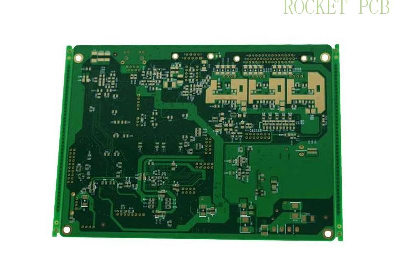
One prominent and reputable company to explore is Rocket PCB when considering PCB prototyping. Rocket PCB is known for its exceptional products and services in circuit board manufacturing. With a diverse range of offerings, including high-speed server boards, large data memory circuit boards, high-frequency hybrid boards, multi-stage HDI boards, IOT modules, and security circuit boards, Rocket PCB caters to various industries such as communication, medical, military, security, industrial, and automotive fields.
Rocket PCB's products have gained recognition and are widely used in domestic markets and internationally, with a strong presence in North America, Europe, Asia Pacific, and other regions. Their commitment to quality, advanced manufacturing capabilities, and expertise in delivering high-performance circuit boards make them reliable for PCB prototyping.
Designers can benefit from their extensive knowledge and experience by partnering with Rocket PCB, ensuring accurate and efficient PCB prototyping processes. Rocket PCB's dedication to customer satisfaction and ability to meet stringent quality standards make them an ideal service provider for your project.
Therefore, we encourage users to explore the offerings and potential of Rocket PCB in their PCB prototyping endeavours. Their wide range of products, global presence, and commitment to excellence make them a trusted partner for delivering exceptional circuit boards that meet the demanding requirements of communication, medical, military, security, industrial, and automotive applications.
Incorporating Rocket PCB into your PCB prototyping journey will empower you to create innovative and reliable designs, enabling your projects to thrive in the competitive market. Trust Rocket PCB to bring your ideas to life with their top-notch products and services, ensuring your success in the circuit board development and assembly process.


