Circuit board factory via technology
by:Rocket PCB
2020-06-14
See a complex PCB circuit boards, such as computer motherboard, may find a few tracks have nowhere else to go, and abruptly terminated.
However, a closer inspection with a magnifying glass, will be in orbit end point shows more details.
Most likely, you'll see it ended up with a small circuit board welding plate, not many larger than the width of the track itself, with one or no hole at its center.
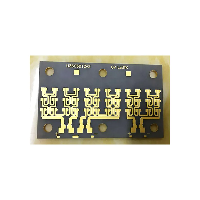
This is said to the circuit board factory via technology.
In fact, orbit not terminated, but continues to travel, although in different layers, hidden under the outermost layers of the PCB circuit boards.
Pad is actually through the end of the pipe insulation material, electrical connection of two parts of the orbit.
In circuit board proofing manufacturers terminology, allowing the track but in different layers of this arrangement is called the PCB hole.
Circuit board proofing manufacturers multi-layer PCB circuit boards using different types of hole for a variety of purposes.
There may be in the same circuit board hole hole, blind hole and into a hole.
Although all pore structure are the same, but their name depends on the origin and termination of layer.
For example, from the most outer layer, across the board and terminates as the outermost hole is another hole.
In the process of its across the board layer, depending on the necessity of the circuit, it can be connected or not connected to the middle tier.
PCB/PCB blind hole from one of the most outer layer, ending but in the middle tier, so only visible on the starting layer.
It may or may not connect to other layers of meantime.
Either from the outermost layer can't see into the hole, because it originated as a lining and ended in another inner layer, can connect with other layers.
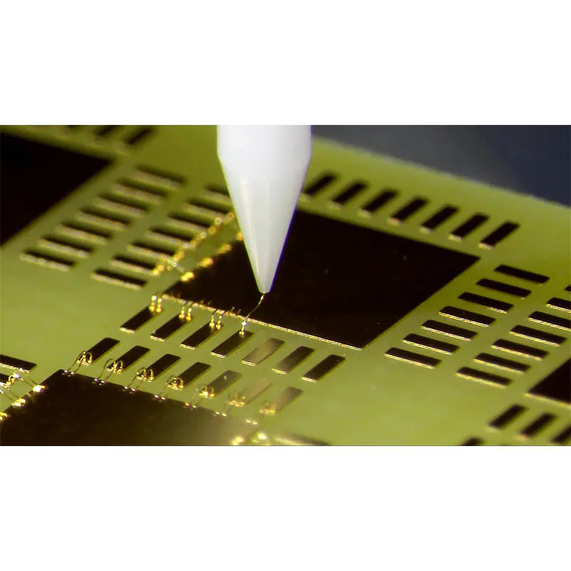
By design, hole by two external bonding pad and an electrical connection of the copper tube.
Two external bonding pad on the PCB circuit boards of initial layer and termination, and all the bonding pad on the middle tier allows copper pipe on the layer with the layers by electrical isolation circuit.
Although two external bonding pad and the pad is part of the layout design, circuit board proofing manufacturer etched onto the PCB circuit board, but the electrodeposition process to form a copper tube that connects the two.
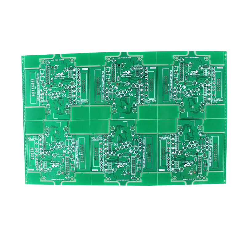
Although in conventional PCB PCB, may find the hole, but the less likely in high density interconnect or HDI PCB.
Rocket PCB Solution Ltd. as one who also teaches operations about how we use our whole operating system as a way to gain advantage and create considerable value and capture value in a sector where, in essence, the environment is quite hostile from a competitive point of view.
As manufacturers we are determined to be the very best in pcb making service, regardless of the size, pedigree or inclinations of our competitors.
Rocket PCB Solution Ltd.’s mission is to provide you with an outstanding member/Customer benefit that helps you meet your organization’s objectives.
When it comes to pcb making service pcb manufacturing services, Rocket PCB Solution Ltd. is the name to reckon with. Not only are they best, they are the most experienced as well and provide wide range of services as well as products at affordable prices. Find out more information on Rocket PCB .
Custom message