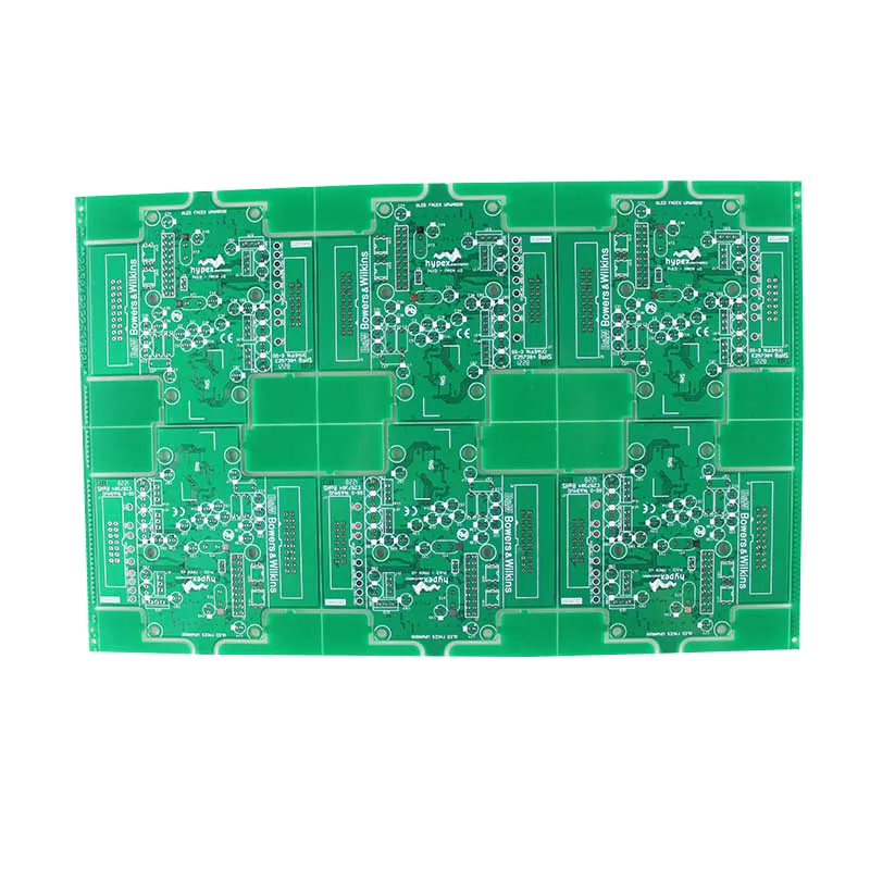
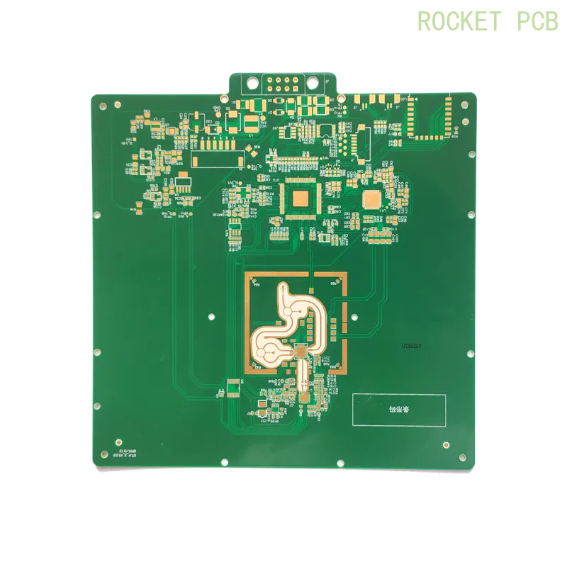
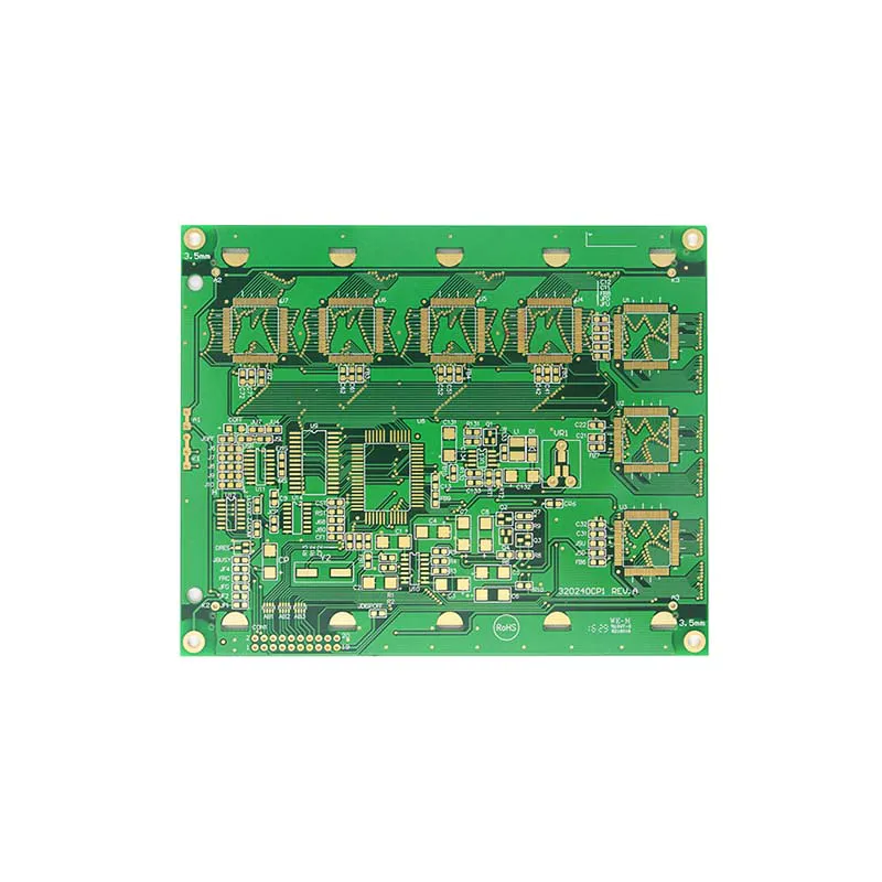
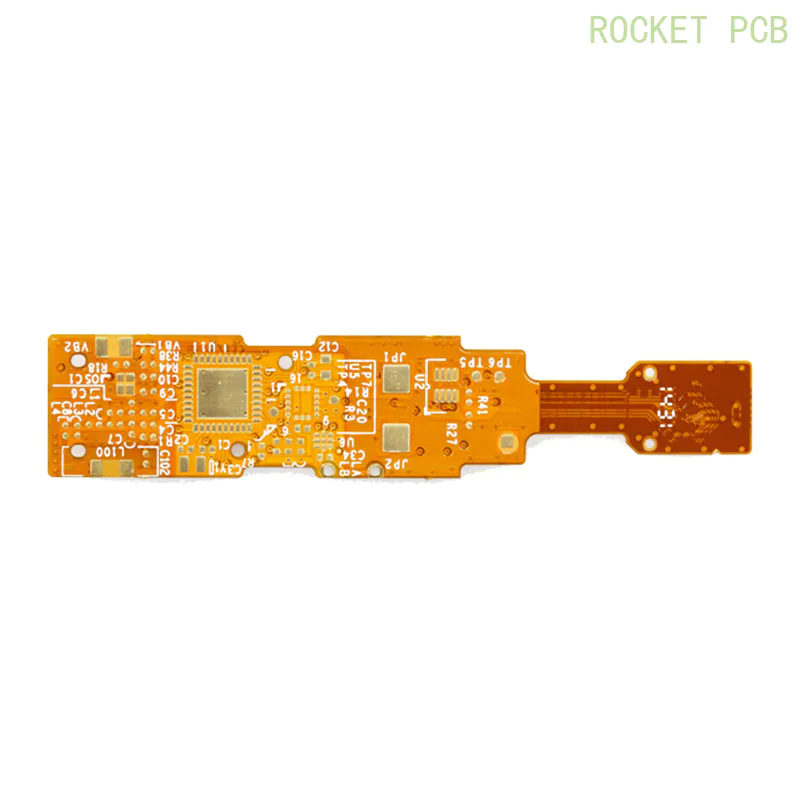
Circuit board copper clad not do more harm than good or more harm than good
by:Rocket PCB
2020-06-08
Copper clad as an important link in PCB circuit board design, do you understand?
A copper clad, is unused space on PCB as datum, then filled with a solid copper, the copper copper area is known as irrigation.
Copper clad significance lies in: reduce ground impedance, improve the anti-interference ability;
Lower pressure drop, and improve the power efficiency;
Connected to the ground, but also can reduce the loop area, etc.
Copper clad copper clad way generally there are two basic ways, is a large area of copper clad (
Solid copper clad)
Copper and grid, that is a good or large area of copper clad copper grid?
Not good, they each have advantages and disadvantages.
1, solid copper clad advantages: have the dual role of increasing current and shielding.
Disadvantages: if the wave soldering, the board may become warped, even bubbles.
Solution: in general, will open a few slots, alleviate blister copper foil.
2, grid, copper clad advantages: from the perspective of heat dissipation, the grid is good,
It reduces the heating surface of copper)
And have played an important role in certain electromagnetic shielding.
Weakness: the simple grid apply copper shield effect, mainly increase the current function is decreased.
The pros and cons of thick copper clad copper circuit board PCB: the inner signal to provide additional shielding protection and noise suppression.
Improve the cooling ability of PCB.
In the process of PCB circuit board production, save the dosage of the etchant.
Avoid caused by uneven copper foil stress at the exit of reflow soldering PCB PCB case become warped deformation caused by different.
Cons: copper outer plane will be the surface components and signal separation of fragmented, if you have bad earth copper foil (
Especially the finely long broken copper)
, it will become the antenna, EMI problems.
If the copper clad for electronic components pin all connection, will cause the heat lost too fast, and difficult to repair welding caused desoldering.
Copper outer plane must be good grounding, need more played hole connected to the main ground plane, a hole to play much, will inevitably affect the wiring channel, unless you use blind holes.
Copper clad attention of engineers in copper clad copper to make to achieve the desired effect, need to pay attention to the following aspects: 1, the single point of different ground connection, it is through 0 the resistance or inductance connection or magnetic beads.
2, equipment internal metal, such as metal heat sink, metal reinforcing bar, etc. , must achieve 'well grounded'.
3, a lonely island,
Dead zones)
Problem, if you feel a lot, then define a pass hole added to also do not cost much.
4, multilayer circuit board layer empty expanse of wiring, not copper clad.
Because it's hard to do you make the copper clad 'well grounded'.
The copper clad near 5, crystals, crystal vibration in the circuit is a high frequency source, it is around copper crystals, then put the crystal vibration of the shell shall be grounded.
Multilayer PCB/gold finger circuit board in June and, at the beginning of the wiring to earth alike, ground walk the line when it should go, can't rely on by adding a hole after the copper clad to eliminate for the connection to pin, the effect is very bad.
7, the PCB board is best not to have sharp horns appear (
<
= 180 degrees)
Because in terms of electromagnetism, it is composed of a transmitting antenna!
For the other there is always a is only big or small, it is recommended to use along the arc of the edge.
8, if PCB circuit board is more, have SGND, AGND, GND, etc. , will be depending on the position of PCB board face, respectively to the main 'to' independent copper clad as reference point, to digital and analog to separate copper from a few words, at the same time before the copper clad, first of all, bold corresponding power cords: 5.
0V、3.
3 v, etc. , as a result, it has formed the different shape of deformation structure.
Conclusion: apply copper on the PCB circuit board, if the grounding problem to deal with, is not do more harm than good, it can reduce signal backflow area, reducing the signal to external electromagnetic interference.
pcb manufacturing services pcb making service is generally used to pcb manufacturing services.
What are you waiting for? Don't you want to provide perfect support to pcb manufacturing services? If yes, so, switch to pcb making service right away!
pcb making service is produced by Rocket PCB Solution Ltd.’s professional skills in high technology.
So, what's a manufacturer to do? Familiarize ourselves with producing pcb making service in various technologies.
Rocket PCB Solution Ltd. has never conceded on the quality and the services of the products which provided to the customer.
Custom message


