
English


Typical Index | Typical value |
Layers | ≤20 |
Size | ≤247*446mm |
Total Thickness | ≤4.0 mm |
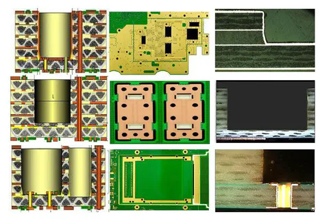
Cavity types | A. Edge plating (PTH plugging, no SM on cavity bottom) B. No plating on edge +no pattern on bottom C. No plating on edge +pattern on bottom (PTH plugging) +SM on bottom |
Cavity Size | 3mm*7mm—200mm*200mm |
Cavity depth | ≤2.0mm |
Surface treatment | HAL not applicable |
Application | Communication, PA, RF |
The high-speed communication demand lower loss(a), smaller delay and lower distortion in signal transmission, which requires PCB using material with excellent Dk&Df, as well as high impedance accuracy. With 1.00053Dk, which is surely higher to vacuum, air cavity in PCB would show higher signal transmission speed, lower distortion and smaller delay. Several air cavities were embedded into different layer of the multi-layer PCB with different low flow resin and mask material.
The main advantages of cavity PCB & PCB cavity are as follows
Improve the overall performance of the product
Increase the density of product assembly
Meet the high-speed and high-information requirements of communication products
Reduce the size and weight of products
Strengthen the safety of surface components
Increase the heat dissipation area
Stepstair PCB& cavity PCB can be divided into
PTH cavity
NPTH cavity
half-PTH cavity (pattern on bottom)
QUICK LINKS
CONTACT US
Office: (+86) 755 23040566
Tel: (+86) 158 9965 5195
E-mail: sales@rocket-pcb.com
Skype: Hans@Rocket-PCB
Whatsapp: 86 1589965 5195
Office Address: 301 Building/B, Huafeng Digital Technology Industrial Park, Chaoyang Ro, Yanchuan, Songgang,518105 Shenzhen, China.
Plant ADD.: No 69, Lianfeng North Road, Xianxi Area, ChangAn Town, Dongguan, China.


