Latest products
what is single sided pcb and multilayer pcb?
by:Rocket PCB
2019-11-26
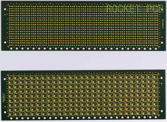
For single-sided PCB, the assembly is on one side, the wire is on the other side, and single-sided PCB is the simplest and most basic circuit board.
With the emergence of electronic transistors, a single panel was developed in early 1950, mainly made in the United States.
The single-sided circuit board was manufactured directly by copper etching at that time.
During the period from 1953 to 1955, Japan used imported copper to manufacture paper-based phenolic copper substrates, which were mainly used in radio products.
In 1956, with the emergence of professional PCB manufacturers in Japan, single-sided circuit board technology has made great progress.
In the early stage, the copper substrate mainly used paper phenol, but due to factors such as low paper phenol electric insulation, poor welding thermal stability and torsion problems, epoxy resin and glass fiber epoxy resin were developed soon.
At present, paper epoxy resin is widely used in consumer electronic products.
Printed circuit board manufacturers have basically no challenge in producing single-sided PCB, and now the technology is quite mature.
How to control production costs and save more costs for customers is the focus of board manufacturers.
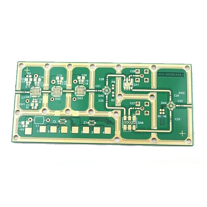
A multi-layer PCB consists of a conductive layer of three or more layers (
Copper foil layer)
These are laminated together to form a multi-layer circuit board.
PP for copper foil layer (prepreg)
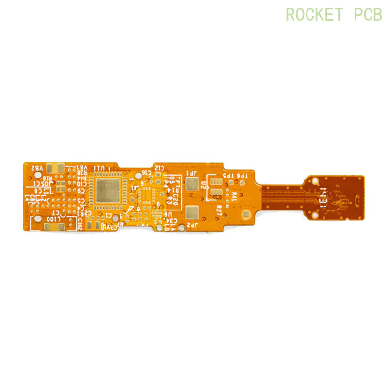
Multi-layer circuit boards are one of the most complex types of printed circuit boards.
Due to the complex PCB manufacturing process, low yield and difficulty of rework, the price is relatively high.
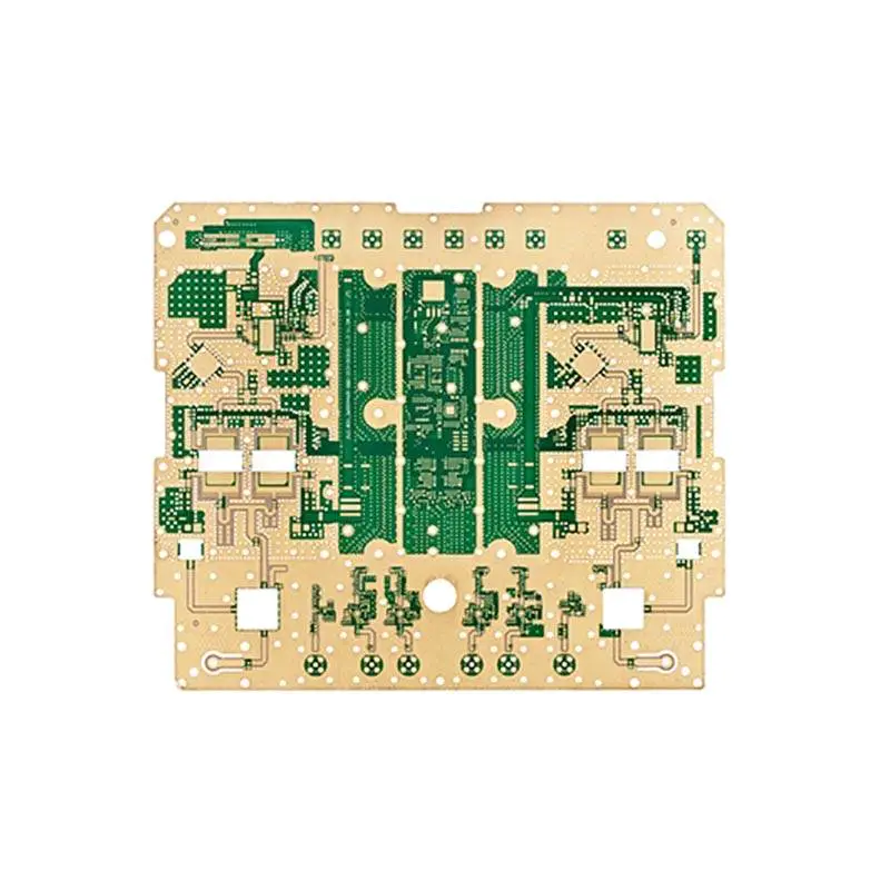
Due to the increase in the density of integrated circuit packaging, the interconnect is highly concentrated, so multi-layer circuit boards need to be used.
In the layout of the printed circuit board, there are sometimes some unforeseen design problems, such as noise, parasitic capacitance, crosstalk, etc. Therefore, when designing the printed circuit board, efforts must be made to make the length of the signal wire as short as possible, avoiding parallel circuits, etc.
Obviously, due to the limited number of cross-circuits, it is difficult to get a satisfactory solution from single-sided PCB or even double-sided PCB.
Under the demand of large-scale interconnect and internet connection, the printed circuit board must be extended to more than two layers to achieve satisfactory performance, so that there is a multi-layer PCB.
The multi-layer PCB has at least three conductive layers, two layers on the surface side, and the rest are synthesized inside the insulating part.
The electrical connection between each layer is usually achieved by plating the penetrating hole.
Unless there are special instructions, both the multi-layer PCB and the double-sided PCB are plated through the hole printed circuit board.
With the emergence of electronic transistors, a single panel was developed in early 1950, mainly made in the United States.
The single-sided circuit board was manufactured directly by copper etching at that time.
During the period from 1953 to 1955, Japan used imported copper to manufacture paper-based phenolic copper substrates, which were mainly used in radio products.
In 1956, with the emergence of professional PCB manufacturers in Japan, single-sided circuit board technology has made great progress.
In the early stage, the copper substrate mainly used paper phenol, but due to factors such as low paper phenol electric insulation, poor welding thermal stability and torsion problems, epoxy resin and glass fiber epoxy resin were developed soon.
At present, paper epoxy resin is widely used in consumer electronic products.
Printed circuit board manufacturers have basically no challenge in producing single-sided PCB, and now the technology is quite mature.
How to control production costs and save more costs for customers is the focus of board manufacturers.
A multi-layer PCB consists of a conductive layer of three or more layers (
Copper foil layer)
These are laminated together to form a multi-layer circuit board.
PP for copper foil layer (prepreg)
Multi-layer circuit boards are one of the most complex types of printed circuit boards.
Due to the complex PCB manufacturing process, low yield and difficulty of rework, the price is relatively high.
Due to the increase in the density of integrated circuit packaging, the interconnect is highly concentrated, so multi-layer circuit boards need to be used.
In the layout of the printed circuit board, there are sometimes some unforeseen design problems, such as noise, parasitic capacitance, crosstalk, etc. Therefore, when designing the printed circuit board, efforts must be made to make the length of the signal wire as short as possible, avoiding parallel circuits, etc.
Obviously, due to the limited number of cross-circuits, it is difficult to get a satisfactory solution from single-sided PCB or even double-sided PCB.
Under the demand of large-scale interconnect and internet connection, the printed circuit board must be extended to more than two layers to achieve satisfactory performance, so that there is a multi-layer PCB.
The multi-layer PCB has at least three conductive layers, two layers on the surface side, and the rest are synthesized inside the insulating part.
The electrical connection between each layer is usually achieved by plating the penetrating hole.
Unless there are special instructions, both the multi-layer PCB and the double-sided PCB are plated through the hole printed circuit board.
Custom message