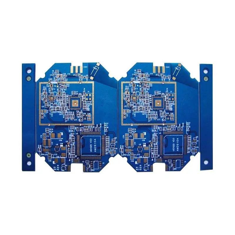
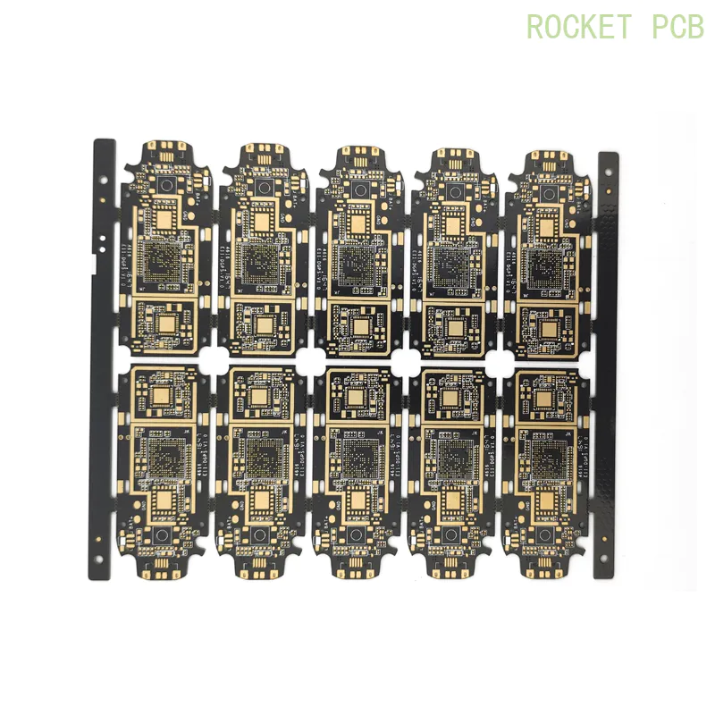
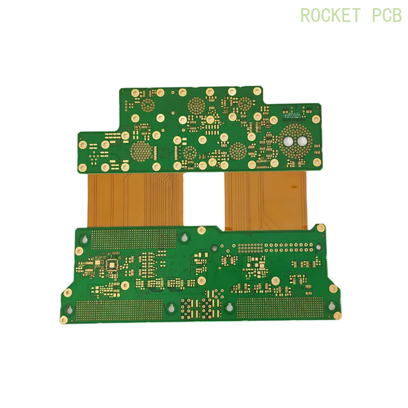
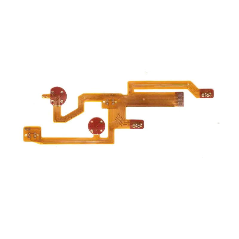
Latest products
what are gerber files for printed circuit boards, and who needs them?
by:Rocket PCB
2019-08-14
When the electronic design engineer completes the circuit design of the application, the next step to complete the product design is to input the schematic details into the computer-based s. . .
When the electronic design engineer completes the circuit design of the application, the next step to complete the product design is to input the schematic details into the computer-based schematic capture program.
Schematic capture program is usually part of electronic design automation, EDA or computer automation design, pcb cad, software design package, will create a network list from the completed schematic, detail each electrical connection between each electronic component.
This network list is used by printed circuit boards or PCB designers in the process of designing printed circuit boards using EDA or pcb cad software.
The completed printed circuit board will provide a physical assembly and interconnect platform for the various electronic components required for the schematic diagram.
The printed circuit board consists of a copper-plated conductive layer etched on one or more layers to form a component pad and interconnect trace, as well as a layer or layer of insulating material (such as epoxy)
Fill the fiberglass to separate the conductive copper layer and provide mechanical strength for the plate.
The single-layer Bureau connects the plate on the upper side of the part and the traces attached to the bottom.
The double board can only have components on the top, or both on the top and bottom of the board, and there are Connection marks on both sides of the board.
The top and bottom of the multi-board have components and traces, as well as many internal layers for interconnect and voltage and ground plane layers.
EDA or pcb cad programs provide details about the design of the complete circuit board in a series of data files for each conductive layer (such as the top, bottom and any internal layer.
The Gerber file format is the standard format for these data files, named after Gerber Scientific Instruments, a pioneer in photoplotter manufacturing.
The original Gerber format conforms to eia rs-
274D standard, consisting of a command file and a tool description file for each conductive layer.
The command file consists of a series of short commands, each followed by a set of X and Y coordinates, which will provide the photo carvers with information to create a graphical representation.
These command files are called Gerber files.
The tool description file or aperture file defines track line width and Dimension Data for all pads and geometry on the layer.
These data files of the computer-generated information of the printed circuit board design are then sent to the printed circuit board manufacturing company in order to manufacture the physical board.
The Gerber file contains the printed circuit board, PCB, computer control machine etching copper layer of the manufacturing plant to create all the information required for assembly pads and connecting tracks, drill all the required holes, and cut the plate to the desired size.
Since the PCB may have a conductive layer from one to more, the old Gerber format eia rs-
274D always assumes a set of command files, one command file per PCB layer, one tool description file or aperture file.
The standard for aperture files has never been established, so each EDA or pcb cad software product has its own version of the aperture file format.
If the aperture file format sent cannot be read by the printed circuit board manufacturer, the aperture information must be re-read
Enter manually.
The newer Gerber format conforms to eia rs-
274X, this format includes aperture information in the header of the file as embedded information for each command or Gerber file.
This new format is often called X-Gerber.
All aperture information is included in the file header, each X-
Gerber file provides all the information you need to make the PCB layer-related part.
The file name of the Gerber file should be descriptive enough for the pcb manufacturer to understand which board and board layer each file applies to, such as membdtop.
Gbr as file name.
The standard process is to include a special README file in each set of files designed by the motherboard.
Define the txt type text file for each file name and its application in board design.
This README will be used by the motherboard vendor.
Use the txt text file as the starting point of the board manufacturing process.
The Gerber file extension is usually. GBR, . GBX, or . ART.
Sometimes extended. TOP and . BOT or . SMT and .
Use SMB instead.
The GB _ type extension.
Usually, a file extension of a file type, top, bottom, screen printing, paste, internal layer, controlled by an EDA or pcb cad package, or optional in a package.
This change in the extension makes it include the README file.
Txt file as the requirements in the overall file package of the motherboard supplier.
The list of documents for the board design will include screen printing at the top, if the assembly is installed on both sides, sometimes the bottom layer, the Assembly placement at the top, and sometimes the bottom layer, welding screen pasting files for surface installation applications, drilling drawings, welding template files, panel drawings, Mat main top and pad main bottom, etc.
For example, the two-sided, monthly, pcb, Jiabao Gerber files will include two front layers, top and bottom, aperture files, if not in RS-
274X format, NC excel on drilling file, drilling tool list file, screen printing file with assembly on each side, welding template file on top and bottom, and the top and bottom screen paste File of the surface mounting plate, if applicable ).
A four-layer board will have all of these files plus two internal layer files and a six-layer board will have all of them plus four internal layer files.
Rocket PCB Solution Ltd. are maintaining a consistent bottom-line profit and that you've shown steady growth over the past few years.
Crazy about products? Rocket PCB Solution Ltd. is the place you must shop at, do visit Rocket PCB Solution to check out our latest collections!
Unlike the , the is more flexibly used in accasions where .
On top of making sure all our day-to-day operations are running smoothly, Rocket PCB Solution Ltd. needs to ensure that we're keeping up with all the quality standards of printed wiring board manufacturers.
Custom message