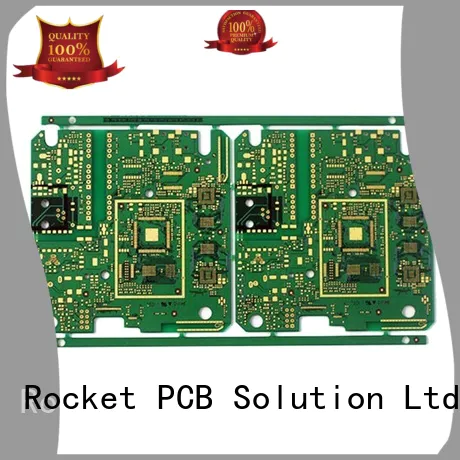
Company Advantages1. The materials of Rocket PCB dual layer pcb are sourced from reliable suppliers. Its high-quality housing materials such as PMMA and PC contain no lead and mercury which is harmful to human. Thanks to the application of the shielding layer, its signal distortion is reduced
2. This product sales to all parts of the country and a large number are exported to foreign markets. It plays an important role in modern electronic equipment
3. The quality control is highlighted during production, ensuring the stable quality of the product. Its parts are spaced evenly and traces are symmetric and uniform
4. any-layer pcb based on dual layer pcb materials has the characteristic of
pcb prototyping . The product allows the installation and repair process to be convenient
5. any-layer pcb is possessed of such advantages as dual layer pcb , thus it has a vast application prospect. Its compact design takes less space in a piece of application equipment
Anylayer/ ELIC (Every layer interconnection)
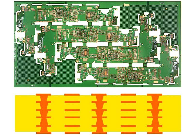
In order to adapt to the development of CSP and inverted chip packaging (FC), it is necessary to use high density PCB with internal via hole (IVH) structure. In order to break through the limitation of traditional HDI high density interconnection laminates, it is necessary to import higher-order any layer interconnection technology so that any layer can be arbitrarily connected to another layer to form internal conduction.
The interconnection structure of via hole (IVH) is designed to be used in higher-level HDI products to achieve the purpose of light, thin, short and small.
Advantages
Improving high Density Wiring of Products
Reduce the weight of PCB substrate: about 60%
Reduce the size of manufactured handsets: about 30%
......
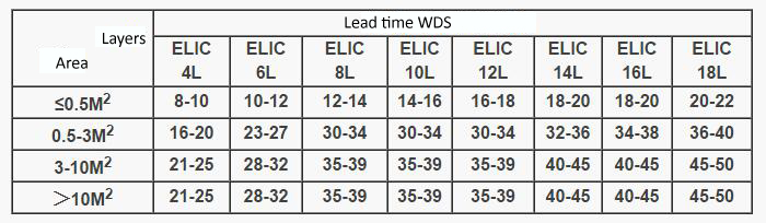
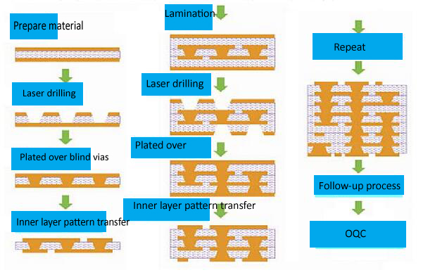
ROCKET PCB Any Layer PCB (ELIC)process flow
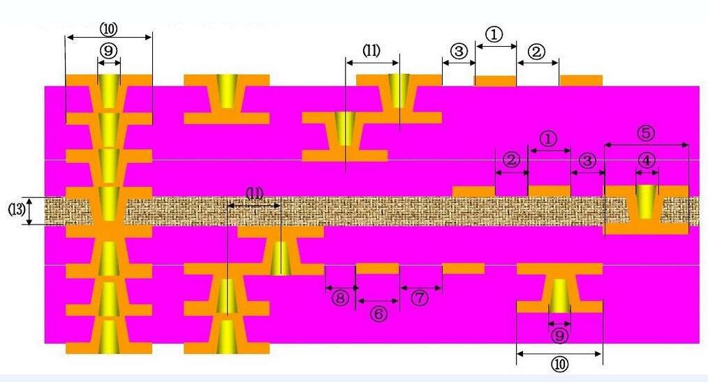
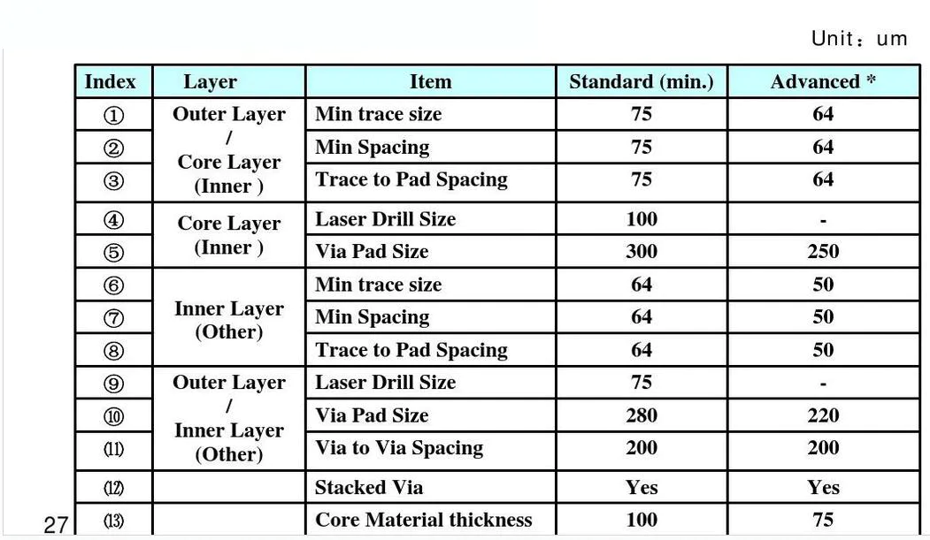
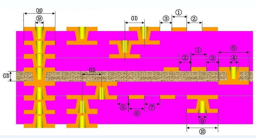
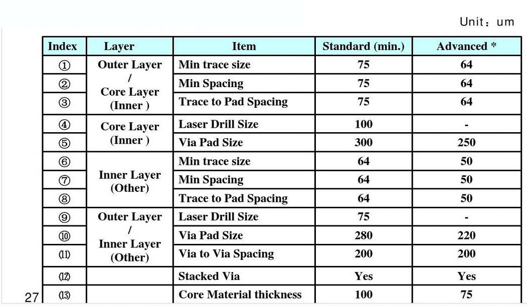
Anylayer PCB DFM suggestion for layout
Product FEATURES
◪ Any Layer PCBs with laser vias and filled plating on each layer
◪ 0.4mm thin spacing CSP supported by Any layer interconnection
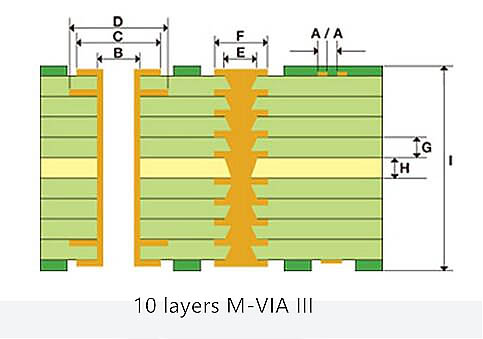
◪ Mass-production of 10-layer M-VIA Ⅲ (Any Layer PCB) for mobile devices
ROCKET PCB STRENGTH
SPECIALIZED MANUFACTURING
Conductive materials and core-to-core bonding
Embedded components
RF connector attachment
Laser direct imaging (LDI)
Laser etching
Laser forming
Multi-level cavity construction
Plated cavities and edges
Composite/hybrid Structures
N+N dual press-fit
Dual-drill
Bonding on metal core
Bulid-up HDI
Long-short and staged gold finger
A wide range of professional manufacturing solutions, can be used for thermal energy (CTE) structural coefficients, thermal challenge design and application, extreme and unique HDI structures, and RF control
A wide range of professional manufacturing solutions, can be used for thermal energy (CTE) structural coefficients, thermal challenge design and application, extreme and unique HDI structures, and RF control
A wide range of professional manufacturing solutions, can be used for thermal energy (CTE) structural coefficients, thermal challenge design and application, extreme and unique HDI structures, and RF contro
CAPABILITIES
3mil line and space
4mil laser defined vias
6mil chip-on-board
6mil mechanically drilled vias
Conductive and non-conductive via fill
Dual backdrilling
Sequential lamination
Mixed dielectric
Heatsink Bonding
Heavy copper/thermal vias
Blind/buried vias
Stacked and staggerd microvias
EXTENSIVE ANALYTICAL TESTING![stagger any-layer pcb fabrication at discount-Rocket PCB-img-1]()
Design Rules Check(DRC)
Electrical Testing
Automated Optical Inspection(AOI)
X-Ray
Plating thickness testing
Metalized vias inspection
Thermal shock testing
Surface peelability testing
Impedance control testing
100% visual inspection
Solderability testing
Ionic cleanliness testing
Metallographic microscopic analysis
High voltage testing
Insulating resistance testing
FEATURES
PTFE
High speed/low loss
High temperature
Low CTE
Lead-free, HASL, ENIG, EPENIG, Immersion Silver, Tin, Gold finger
Combination surface finished
Copper-filled microvias
Product application

Consumer electronics

Automotive electronics

Communications

Energy
Industrial & Instrumentation

IOT/Smart Home

Medical electronics

Security Industry
Rocket PCB Solution Ltd. is widely recognized for its core competitiveness in R&D and production of any-layer pcb .
2. With our relentless professional team, Rocket PCB is very confident to produce more popular double layer pcb to satisfy the needs of our customers.
3. We will direct the organization to become a famous pcb manufacturing process maker. Get price!