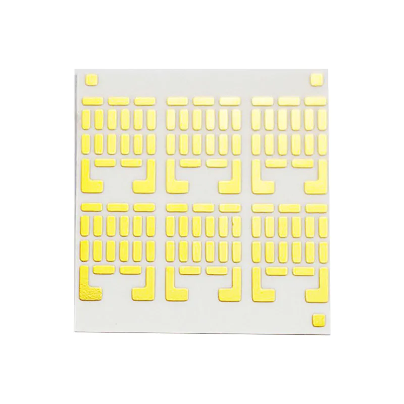
Some defects in the process of multilayer circuit board manufacturing
A poor, multilayer circuit board line etching etching line deformation problem in multilayer circuit board outer line, if the copper foil ridge deep surface resin is quite deep, dense lines after etching area may also have residual copper, these phenomena may be it is not easy to detect after etching, but in the nickel and immersion gold process could be found after the line or the deformation of welding pad edge grow line or metal area. The problem sometimes is considered to be the problem of residual or washed poor, but in fact is a problem of incorrect line or copper etching. In figure 9. 9, for typical etching process line caused by the deformation. In figure 9. 9 (2) peel tin bad may cause gold surface dew copper etching after peeling tin must note that whether stripping was left unfinished light gray medium metal exists. If it does not remove clean brush grinding, pickling and micro erosion may not be able to completely remove and this will inhibit nickel gold leaching reaction started, if the response is likely to be completely unable to start produce gold-plated copper surface leakage phenomenon. Three, the problem of residual copper copper through distributed wall are not copper hole, mainly is the overall copper plating for etching after remove, or bore with cover process not let tin plating, etching after remove copper. But have no way to remove palladium metal etching liquid and, therefore nickel gold will still be in the process of adsorption on the hole wall. For the hole wall don't metal products, this is a direct. SSD multilayer circuit board there are some multilayer circuit board manufacturers to launch the so-called no chemical nickel gold leaching of chemical copper, a simple approach is to reduce the concentration of the metal palladium, borrow this to make the subsequent cannot quickly and plating nickel gold, and therefore no copper hole can reduce production. But this approach will have insufficient chemical copper activity and hole to break the potential crisis, in the operation of the chemical copper aspects will be narrowed down. Also have manufacturers use in addition to the practice of palladium, increase after peeling tin slot in addition to the palladium solution treatment, but it must be increased in the current process of liquid tank Settings, operating costs will increase. At the same time, most in addition to the palladium system are in danger of erosion of copper, and some of the so-called special yao and of the cost of the patent and water. Another approach is to before peeling tin mercaptan kind of palladium layer passivation solution hole, make later nickel and immersion gold process cannot function. But mercaptan processing if flushing impurity, residue will into peel tin bath makes on the copper surface sulfide. On the surface of the copper sulfide nickel reaction is fatal, thus to prevent dew copper problem is very difficult. Therefore, at present in the absence of copper in hole exact solution is still in development. In figure 9. 10, as the typical example of soldering pad dew copper. Basically copper surface without inadequate activity, is likely to be alone on the surface of the copper pad electronegative is still not strong not rev or plated surface caused by pollution has been unable to response. In figure 9. 10