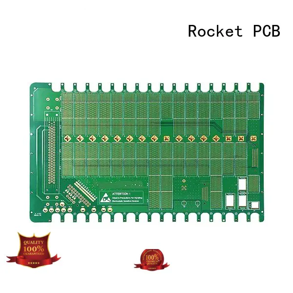
PCB Backplane Technology
The backplane has always been a
specialized product in the PCB manufacturing industry, the backplane is
thicker and heavier than the conventional PCB board, and its heat
capacity is larger accordingly.
In
view of the slow cooling speed of the backplane, the length of the
reflow weld furnace should be lengthened. There is also a need for
forced air cooling at the outlet to reduce the backplane temperature to a
safe operating level.
The user's need for thinner cores and more layers of backplane comes to the opposite requirements of the conveyor system. When a large power application card is plugged into the backplane, the copper layer thickness must be moderate to provide the required current,all of these factors lead to an increase in the average weight of the backplane. This requires that conveyor belts and other conveyor systems must not only be able to safely transfer large-size raw material backplanes, and it must also be taken the weight increment into account.
Because the backplane is thicker than the conventional PCB, and the number of holes is much more, it is easy to cause the outflow phenomenon of processing fluid. In order to minimize the amount of liquid carrying and remove the possibility of any impurities remaining at the through hole, it is very important to clean the hole by means of high-pressure flushing and air blower.
Interlayer alignment become important due to the increasing number of layers required by user applications. Interlayer-to-bit requirements tolerance convergence, larger backplane size makes this convergence more demanding.
All pattern processes are produced in a controlled environment of a certain temperature and humidity. The alignment tolerance of the entire area before and after the graph should be maintained at 0.0125mm. CCD camera needs to be used to complete the front and rear layout of the position. After etching, use four drilling system to perforated the inner laminates. Perforated through the core board, position accuracy maintained at 0.025mm, the repeatable capacity of 0.0125mm, then insert the perforation with the pin, align the etched inner layer, At the same time glue the inner layer together. The use of this etched perforation method can fully ensure that the hole and etching copper plate alignment, forming a solid ring design structure. However, with the user in the PCB wiring requirements more detailed, in order to keep the board cost unchanged, the etching copper plate size is required to be smaller, thus requiring better alignment of the interlayer copper plate. Fixture and conveyor equipment must be able to transmit large plates and heavy plates simultaneously.
In addition to drilling requirements, backplane designers generally
have different requirements for copper uniformity on the surface of the
outer layer Some designs etch very few signal lines on the outer layer.
On the other hand, in the face of high-speed data rate and impedance
control line requirements, the external layer set solid copper sheet
will become very necessary for the use of EMC shielding layer
Etching
line widths, thicknesses, and tolerances become key indicators for the
effectiveness and repeatable control of the backplane impedance. At this
point, the AOI method can be used to ensure that the etched copper
pattern matches the design data. The impedance model is used to
determine and control the sensitivity of the impedance to the line width
change by setting the line width tolerance on the AOI.
Traditionally, for reliability reasons, there is a tendency to use passive components on the Backplane. However, in order to maintain the fixed cost of active plate, BGA and other active devices are more and more designed on the Backplane, component mounting equipment must not only be able to place smaller specifications of capacitors and resistors but also be able to operate on additional silicon packaging components. In addition, the Backplane large specification requires the installation of equipment bed to be large, and the heavy backplane can also be shifted with fine position tolerances.
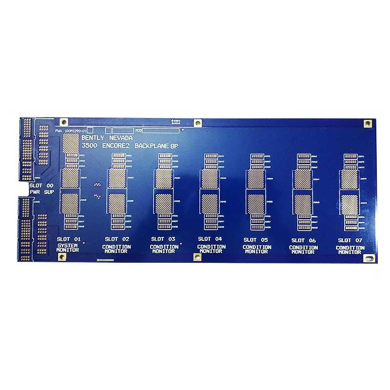
◪ Panel sizes up to 54 inches
◪ Over 70 layers
◪ Blind and back drilled through holes
◪ Dual diameter holes
◪ Heavy copper layers
◪ Connector expertise







Copyright © 2026 Rocket PCB Solution Ltd. | All Rights Reserved Sitemap Friendship link: CNC machining heat sink