


One Article Understanding Ceramic PCB Board Packaging
One Article Understanding Ceramic PCB Board Packaging
1. What is a PCB package?
The PCB package defines the physical interface between electronic components and the PCB, and provides the necessary information for PCB assembly and maintenance, such as the shape and symbol of the component, the number of pads, location, reference pins, polarity, etc.
Each component placed on the side of the PCB must have its own package, including the copper area on the PCB where the component will be soldered. For example, a 16-pin SSOP package cont
ains 2 rows of 8 rectangular pads each. The figure below shows the footprint of a common electronic component in a 16-pin SSOP package. The red part corresponds to the copper area on the layer, while the other colors represent the mechanical type layer. There are many types of common PCB packages (1). SOP (Small Outline Package).
The smallest footprint used for integrated circuits (ICs), usually about 0.4 inches x 0.4 inches. (2). QFP (Quad Flat Package) A larger PCB footprint used for ICs and integrated circuits, usually about 0.8" x 0.8", but can also be as large as 1" x 1". (3) BGA (Ball Grid Array). This is a larger PCB package for ICs and integrated circuits with many connections. It is usually rectangular with pins on all four sides, allowing them to be placed in any orientation. Sizes vary widely, depending on the number of connections per IC; sizes range from 0.5" x 0.5" to over 2" x 2".

Picture:SSOP Package Example
2. Disadvantages of ordinary PCB packaging
Ordinary printed circuit board (PCB) materials have low thermal conductivity and poor heat dissipation performance, making them difficult to use for packaging high-power devices. Long-term operation of electronic components in high-temperature environments will lead to deterioration of their performance and even damage of the devices. As electronic packaging technology continues to develop in the direction of miniaturization, high density, multi-function and high reliability, the power density of electronic systems is getting higher and higher, and the heat dissipation problem is becoming more and more serious. The continuous increase in the input power of electronic components and the large dissipation power bring newer and higher requirements for heat generation. For high-power products, the packaged PCB is required to have high electrical insulation, high thermal conductivity, and thermal expansion coefficient matching the chip.
Therefore, effective electronic packaging requires continuous improvement of the performance of packaging materials and rationalization of electronic circuit wiring, so that electronic components can achieve good heat dissipation while being unaffected by the environment, helping the electronic system maintain good stability
3. Classification of electronic packaging
Electronic packaging can generally be classified according to packaging structure, packaging form and material composition. From the perspective of packaging structure, it mainly includes substrate wiring, interlayer dielectric and sealing material substrate. The substrate is divided into rigid board and flexible board. The interlayer dielectric is divided into organic polymer (polymer) and inorganic (silicon oxide, silicon nitride and glass) to protect the circuit, isolate and insulate, and prevent signal distortion. The sealing material is currently mainly epoxy resin, accounting for more than 97% of the entire electronic sealing material. Epoxy resin has low cost, large output and simple process. From the perspective of packaging form, it can be divided into airtight packaging and solid packaging. Airtight packaging means that there is a certain gas space around the tube core in the cavity to isolate it from the outside world, and solid packaging means that the tube core and the packaging cavity form a whole entity. From the perspective of material composition, it is mainly divided into metal-based, ceramic-based and plastic-based packaging materials.
4. Advantages of ceramic packaging
Ceramic packaging has great development potential in high-precision sealing. Ceramic packaging is an airtight packaging. The main materials are Al2O3, AIN, BeO and mullite. It has the advantages of good moisture resistance, high mechanical strength, small thermal expansion coefficient and high thermal conductivity. The main materials of metal packaging include Cu, Al, Mo, W, W/Cu and Mo/Cu alloys, which have the advantages of high mechanical strength and excellent heat dissipation performance. The main materials used for plastic packaging are thermosetting plastics, including phenolic, polyester, epoxy and silicone, which have the advantages of low price, light weight and good insulation performance. In addition, four major composite materials are commonly used in electronic packaging, namely polymer matrix composite materials (PMC), metal matrix composite materials (MMC), carbon/carbon composite materials (CCC) and ceramic matrix composite materials (CMC).
Ceramic PCB board packaging has many advantages such as withstanding high temperature and facilitating analysis of functional abnormalities after circuit tape-out. It can effectively improve the heat dissipation performance of high-power electronic devices and meet the application requirements of power device packaging. With the development of various electronic products, ceramic PCB board packaging applications are becoming more and more extensive.
5. Packaging materials (taking the LED industry as an example)
Resin-based packaging PCB: high supporting costs and difficult to popularize
EMC and SMC have high requirements for compression molding equipment. The price of a compression molding production line is about 10 million yuan, and it is difficult to popularize on a large scale.
The patch-type LED brackets that have emerged in recent years generally use high-temperature modified engineering plastics, with PPA (polyphthalamide) resin as raw material. By adding modified fillers to enhance certain physical and chemical properties of PPA raw materials, PPA materials are more suitable for injection molding and patch-type LED brackets. PPA plastic has very low thermal conductivity, and its heat dissipation is mainly carried out through the metal lead frame. The heat dissipation capacity is limited and it is only suitable for low-power LED packaging.
Metal core printed circuit board: complex manufacturing process and few practical applications
The processing and manufacturing process of aluminum-based PCB is complex and costly. The thermal expansion coefficient of aluminum is quite different from that of chip materials, so it is rarely used in practical applications. Most high-power LED packages use this type of PCB, and its price is between medium and high prices.
The high-power LED heat dissipation PCB currently used in production has an extremely low thermal conductivity of the insulation layer, and due to the existence of the insulation layer, it cannot withstand high-temperature welding, which limits the optimization of the packaging structure and is not conducive to LED heat dissipation.
Silicon-based packaged PCB: facing challenges, yield rate is less than 60%
Silicon-based PCB faces challenges in the preparation of insulation layer, metal layer and via, and the yield rate does not exceed 60%. Silicon-based materials are used as LED package PCB technology in the semiconductor industry and LED industry. The thermal conductivity and thermal expansion properties of silicon-based PCBs show that silicon is a packaging material that matches LEDs better. The thermal conductivity of silicon is 140W/m·K. When applied to LED packaging, the thermal resistance is only 0.66K/W; and silicon-based materials have been widely used in semiconductor processes and related packaging fields, and the related equipment and materials involved are quite mature. Therefore, if silicon is made into LED package PCB, it is easy to form mass production.
However, there are still many technical problems in LED silicon PCB packaging. For example, in terms of materials, silicon materials are easy to break, and there are also problems with structural strength. In terms of structure, although silicon is an excellent thermal conductor, it has poor insulation and must be oxidized and insulated. In addition, its metal layer needs to be prepared by sputtering combined with electroplating, and the conductive holes need to be made by corrosion. In general, the preparation of the insulating layer, metal layer, and vias all face challenges, and the yield rate is not high.
Ceramic package PCB: Improve heat dissipation efficiency to meet the needs of high-power LEDs
The high thermal conductivity ceramic substrate significantly improves the heat dissipation efficiency and is the most suitable product for the development needs of high-power, small-size LEDs. Ceramic PCBs have new thermal conductive materials and new internal structures, which make up for the defects of aluminum metal PCBs, thereby improving the overall heat dissipation effect of PCBs. Among the ceramic materials currently available for heat dissipation PCBs, although BeO has a high thermal conductivity, its linear expansion coefficient is very different from that of silicon, and it is toxic during manufacturing, which limits its application; BN has good comprehensive performance, but as a PCB material, it has no outstanding advantages and is expensive. It is currently only under research and promotion; Silicon carbide has high strength and high thermal conductivity, but its resistance and insulation withstand voltage values are low. After metallization, the bonding is unstable, which will cause changes in thermal conductivity and dielectric constant, and it is not suitable as an insulating package PCB material. Although Al2O3 ceramic substrate is the most produced and widely used ceramic substrate at present, its thermal expansion coefficient is relatively high compared with Si single crystal, which makes Al2O3 ceramic substrate not very suitable for use in high-frequency, high-power, and ultra-large-scale integrated circuits. A1N crystal has high thermal conductivity and is considered to be an ideal material for the new generation of semiconductor PCBs and packaging.
AlN ceramic PCB has been widely studied and gradually developed since the 1990s. It is currently generally considered to be a promising electronic ceramic packaging material. The heat dissipation efficiency of AlN ceramic PCB is 7 times that of Al2O3. The heat dissipation benefit of AlN ceramic PCB applied to high-power LEDs is significant, which greatly improves the service life of LEDs.
Direct copper-bonded ceramic board (DBC) developed based on on-board packaging technology is also a ceramic PCB with excellent thermal conductivity. DBC does not use adhesives in the preparation process, so it has good thermal conductivity, high strength, strong insulation, and a thermal expansion coefficient that matches semiconductor materials such as Si. However, ceramic PCBs have low reactivity with metal materials, poor wettability, and are difficult to implement metallization. It is not easy to solve the problem of micropores between Al2O3 and copper plates, which makes the mass production and yield rate of this product a great challenge, and it is still the focus of research by domestic and foreign researchers. At present, only a few companies led by Slitun can mass produce it in China.
DPC ceramic PCB is also known as direct copper-plated ceramic board. DPC products have the characteristics of high circuit accuracy and high surface flatness. They are very suitable for LED flip chip/eutectic process. With high thermal conductivity ceramic substrate, the heat dissipation efficiency is significantly improved. It is a cross-era product that is most suitable for the development needs of high-power and small-size LEDs.
6. The main forms of ceramic PCB board
Currently, the main forms of ceramic packaging include ceramic dual in-line package CDIP, ceramic pin grid array CPGA, glass seal (CerDIP, which has been gradually replaced by ceramic dual in-line package and is not often used because it requires electroplating during the packaging process, which prolongs the process time), ceramic leadless carrier CLCC, ceramic quad flat CQFP, ceramic quad leadless shell CQFN, ceramic flat CFP, etc.
7. What information does the ceramic PCB package contain?
(1) Pad/hole
It is used to indicate the position of the pad for assembling SMD components or the hole for fixing through-hole components. This is crucial for welding and must be accurately defined.
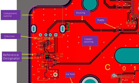
(2) Component outline
It can be defined as the protection area of the PCB package. Other components can be placed in this area. This boundary defines the entire body of the component and is responsible for defining the main layer of the component shape.
(3) Reference designator
This is an alphanumeric code that uniquely identifies components in schematics and PCB layouts. The following figure shows some reference designators, such as R3 resistor and C5 capacitor.

(4) Pin 1 indicator
When placing components with a large number of pins, such as integrated circuits, it is important to indicate the location of pin 1 on the package to avoid possible misunderstandings during the assembly phase. This is the case, for example, with components with QFP or DIP packages. It can be a white circle, a triangle, or a square, as shown below.

Triangle flag pin 1

(5) Mechanical information
Some components may have some mechanical parts, or protrusions that may extend over other components, creating possible collisions or overlaps between components. For example, a heat sink.
(6) 3D models and symbols
Each PCB package has an associated symbol in the schematic and, in most cases, an associated 3D model. This enables designers to create a 3D model of the entire board and verify the correct positioning and mutual distances between components.
8. Packaging process (taking the packaging of optical modules as an example)
The main packaging processes of OSA and ROSA include TO coaxial packaging, butterfly packaging, COB packaging and BOX packaging. TO coaxial packaging is mostly cylindrical, with the characteristics of small size, low cost and simple process, suitable for short-distance transmission, but it also has disadvantages such as heat dissipation difficulties. Butterfly packaging is mainly a cuboid, with a complex design structure, large shell area, good heat dissipation, and suitable for long-distance transmission. COB is a chip-on-board packaging, which attaches the chip to the PCB board to achieve miniaturization, lightness and low cost. BOX packaging is a butterfly packaging used for multi-channel parallelism. In addition, other common packaging methods include dual in-line package (DIP), leadless chip carrier (LCC), etc.
TO package: One of the plug-in packages, consisting of a TO tube seat and a TO tube cap. The TO tube seat serves as the base of the package component and provides it with power, while the tube cap can achieve smooth optical signal transmission. These two components form a sealed package to protect sensitive components.
DIP: One of the plug-in packages, the pins are led out from both sides of the package, and can be directly soldered on a chip socket with a DIP structure, or soldered in a soldering position with the same number of solder holes. Its characteristics are that it can easily realize the perforation soldering of the PCB board, and it has good compatibility with the motherboard. The packaging materials are plastic and ceramic.
PGA: One of the plug-in packages, the vertical pins on its bottom are arranged in a display shape. The package substrate basically uses a multilayer ceramic substrate. It is used for high-speed large-scale logic LSI circuits. There are generally two types: CPGA (ceramic pin grid array package) and PPGA (plastic pin grid array package).
SOP: It is a surface mount package, and the pins are led out from both sides of the package in a seagull wing shape. Common packaging materials include: plastic, ceramic, glass, metal, etc., and currently TSOP, VSOP and other forms have been developed.
LCC: One of the surface mount packages, the pins are led out from the four sides of the package. It is a package for high-speed and high-frequency ICs. According to different materials, it is further divided into PLCC (plastic package) and CLCC (ceramic package).
BGA: One of the surface mount packages. Ball bumps are made on the back of the printed circuit board in an array to replace the pins. The LSI chip is assembled on the front of the printed circuit board, and then sealed with molded resin or potting methods. It can be further divided into PBGA, CBGA, etc.
CSP: CSP packaging can make the chip area and package area close to the ideal situation of 1:1. Compared with BGA packaging, CSP packaging can increase the storage capacity by three times in the same space. It has the advantages of small size, large number of input/output terminals and good electrical performance.
COB: It is one of the bare chip mounting technologies. The semiconductor chip is mounted on the printed circuit board. The electrical connection between the chip and the substrate is achieved by wire stitching and covered with resin to ensure reliability. COB is the simplest bare chip mounting technology, but the packaging density is poor.
TO coaxial package laser schematic diagram

Schematic diagram of butterfly package laser

BOX package receiver diagram


