
English


|
Typical Index |
Design Features |
|
Layers |
42 |
|
Size |
24.2”×36.2” |
|
Total Thickness |
0.327” |
|
Min. DHS |
0.023” |
|
A/R |
14.2:1 |
|
Hole tolerance |
±2mil |
|
Blind via distance |
60mil |
|
Cap copper thk. |
1 Oz |
|
registration |
Layer-Layer 4mil in total 7mil |
|
Base Material |
TU872SLK |
|
Surface treatment |
Imm. Tin |
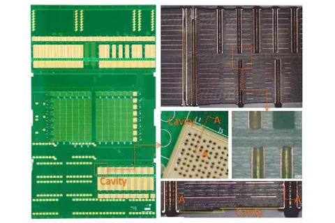
Research Progress of Blind Hole Press-fit backplane
Blind hole press-fit backplane is suitable for press-fit installation of components backplane. Because the press-fit installation connector requires that the mounting hole wall copper on the backplane be clean, compact and wear-resistant. Therefore, the copper thickness of the through hole, the blind hole on the backplane board and the cleanliness of the hole wall are required to be very high. With the renewal of electronic equipment, the requirement for high density of backplane is getting higher and higher, the number of layers of blind hole press-fit PCB backplane is increasing, and the depth of blind hole on it is also increasing, which not only increases the challenge of deep hole electroplating, but also brings difficulties to the cleaning of blind hole after through hole electroplating.
In the production of printed circuit board, blind hole is formed through lamination, and then drilled through hole and metalized through hole. Therefore, when through-hole copper plating, the plating liquid will also enter the blind hole. In the super-high-rise blind hole press-fit backplane, the depth of the blind hole is very high. It is difficult to clean the deep blind hole after the plating liquid enters the deep blind hole. The unclean cleaning of electroplating residual liquid in blind holes will corrode the copper in holes, which will bring long-term reliability risks to the connection of crimping devices.
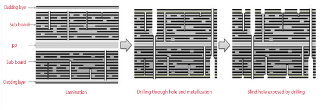
In order to solve the problem of blind hole contamination in high-rise blind hole press-fit backplane PCB, the traditional manufacturing method of high-rise blind hole backplane is the cladding method: in the original PCB design, two copper cladding layers are added up and down as the protective layer.
First, the original PCB design part is made. After all the blind holes of the design layers are completed, two copper-clad layers are added up and down through pressing. The new copper-clad layer shields the original blind holes, then makes through holes and electroplating metallization. In the process of through-hole metallization, the new copper-clad layer protects blind holes and avoids electroplating liquid deposited in deep blind holes will corrode the copper wall and affect the long-term reliability of products.
The process of making blind hole press-fit backboard by cladding method is as follows:
First sub board making (multilayer board) →second sub board making (multilayer board) →lamination→ drilling through hole →electroplating through hole→ drilling blind hole →milling board forming →testing.
Cladding method is the solution of blind hole press-fit method at present. Although this technology adds two layers to the original circuit design, it will not affect the original circuit function, and solve the problem of difficult cleaning of high-level blind hole press-fit backplane PCB board. However, the plating limitation of high thickness-diameter ratio still affects the development of this technology to super-high-rise blind hole press-fit backplane.
Blind-hole press-fit backplane PCB suitable for press-fit installation is the mainstream direction of high-density backplane development. In the future, for example, the rapid development of large-scale electronic equipment such as communication equipment, blind-hole press-fit PCB backplane will be the mainstream product to support the development of its industry.
Rocket-pcb is a few supplier of blind-hole press-fit PCB backplane in China. Backplane technology is far ahead in the industry, supporting a variety of high-precision backplane PCB products and supports all kinds of high-end PCB products.
QUICK LINKS
CONTACT US
Office: (+86) 755 23040566
Tel: (+86) 158 9965 5195
E-mail: sales@rocket-pcb.com
Skype: Hans@Rocket-PCB
Whatsapp: 86 1589965 5195
Office Address: 301 Building/B, Huafeng Digital Technology Industrial Park, Chaoyang Ro, Yanchuan, Songgang,518105 Shenzhen, China.
Plant ADD.: No 69, Lianfeng North Road, Xianxi Area, ChangAn Town, Dongguan, China.


