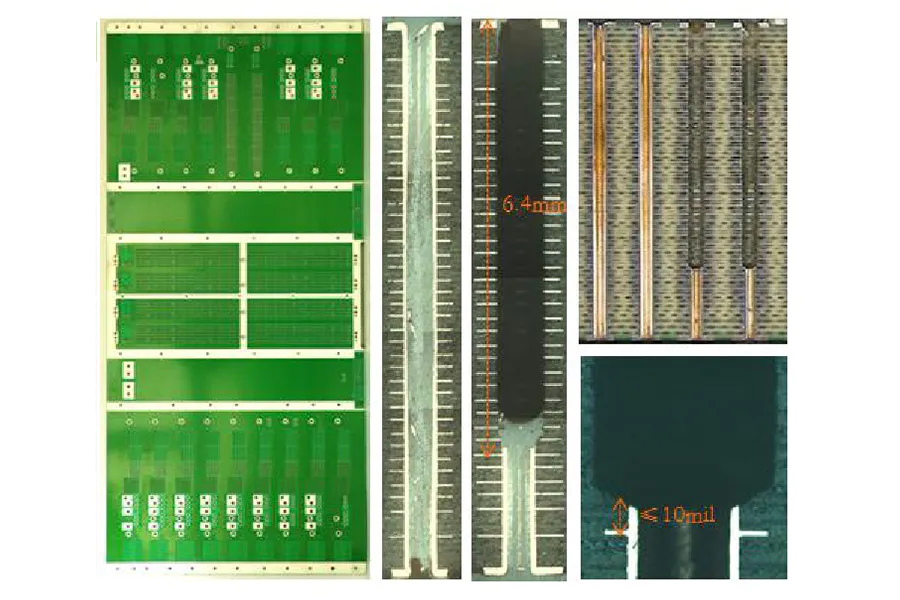
Typical Index | Design Features |
Layers | 38L |
Size | 42.5”×19.8” |
Total Thk. | 0.275” |
DHS | 0.018” |
A/R | 15.3:1 |
Line resolution | IL Hoz:±0.5mil |
Stub | ≤10mil (drilling depth is 6.4mm) |
Base Material | M6 |
Impedance tolerance | ≤8% |
Registration | Same core 3.0mil Adjacent layers 4.0mil In total 6.0mil |
With the data-intensive applications such as large data and cloud computing, the scale of data centers is expanding. The demand for traffic and capacity among data centers, within data centers and within servers/storage has become a huge number. High speed backplane PCB is an important part of data center signal transmission, which mainly provides signal interconnection channels for various sub-cards in the system.
The core indicators of high-speed backplane PCB are signal integrity, namely impedance control, reflection and crosstalk. Therefore, the material of high-speed backplane PCB requires low loss factor enough to reduce signal transmission loss; the thickness of single-layer board is thin, so it can be used for multi-layer board lamination.
High-speed materials are mainly M6 and M7, and now TUC is also good. TU872SLK, TU933, etc., can produce more than 20 layers of PCB. The process control is similar to FR4, but degumming slag needs plasma.
Rocket PCB as China's leading PCB supplier, can process high speed and mixed backplane PCB custom service, can do 10G, 25G, 56G, automotive radar hybrid PCB board.
Design Consideration of High Speed Backplane PCB
As the data rate exceeds 1 Gbps, designers must solve new problems in the design of their backplane systems. The signal integrity of these backplanes is affected by skin effect, dielectric loss, greater noise caused by crosstalk and inter-symbol interference(ISI).
Skin effect is a phenomenon in which most of the current will be concentrated on the external conductor as the frequency increases. The loss caused by skin effect is proportional to the square root of frequency, the width and height of the line.
Dielectric loss is caused by thermal loss of board dielectrics and increases linearly with frequency. At higher frequencies, dielectric loss becomes a serious problem. These losses not only reduce the amplitude of the signal, but also slow down the edge speed of the signal, resulting in poor signal divergence and jitter tolerance.
The main source of noise is crosstalk caused by high density connector and backplane wiring. Crosstalk is a major noise source caused by high-density connector and backplane layout and wiring
There are two types of crosstalk: near-end crosstalk (NEXT) and far-end crosstalk (FEXT). The signal emitted by the transmitter near the victim receiver interferes with the received signal and causes NEXT. FEXT is caused when the received signal is interfered by a "remote transmitter" connected to the victim receiver. All these channel impairments can be compensated or eliminated by special signal adjustment circuits (such as pre-emphasis and equalization) in backplane interconnection devices. These circuits compensate for signal loss by attenuating low-frequency components and amplifying high-frequency components.
Innovative Signal Adjustment Technology
The key role of backplane interface devices is to solve the channel damage problems such as loss and crosstalk, and thus prolong the service life of backplane. The interface transmitter has signal adjusting circuits such as amplitude control and pre-emphasis.
Similarly, the backplane interface receiver uses equalization technology to control loss. In addition, these devices also require testable features such as JTAG and BIST to enable system-level testing during manufacturing. National Semiconductor's four-way 5Gbps SerDes meets all these requirements.


