
English


Typical Index | Design Features |
Layer | 40 |
Size | 33”×19” |
Total thickness | 0.276” |
1st drill hole size | 0.022” |
2nd drill hole size | 0.018” |
A/R | 12.6:1 |
L/S | 5.0/5.0mil (IL) |
Base material | 370HR |
Surface treatment | Imm. Tin |
Dual Drilling is a kind of drilling processing technology to solve the drilling of thick backplane PCB board, because drilling needs two drilling holes to complete the processing of through-hole, the design of drilling and positioning system, the processing sequence of positive and negative drilling, the design of the size of drilling tool for twice drilling holes all have special requirements
Generally, we call PCB backplane as a PCB board with a thickness of more than 4.0 mm and a typical design of press-fit holes. PCB backplane is characterized by its large size, and it is not uncommon for PCB backplane to have a dimension of more than 1000mm.
Generally 4.0-6.0 mm, sometimes even up to 10.0 mm. In addition, the main holes of PCB backplane are row sockets. Customers have very strict requirements on the dimension tolerance, hole copper quality and even shape of such holes. Due to the limitation of mechanical drilling processing capacity, the drilling technology of PCB backplane is a key factor in the whole process. There are many ways to solve the technical problems of thick PCB backplane drilling, one of which is dual-drilling. Drilling technology can break through the mechanical drilling capacity limit, no need to customize special drill bit can complete the drilling of thick PCB backplane, which has obvious advantages for batch processing of thick PCB backplane.
Some key engineering design techniques on dual-drill backplane PCB
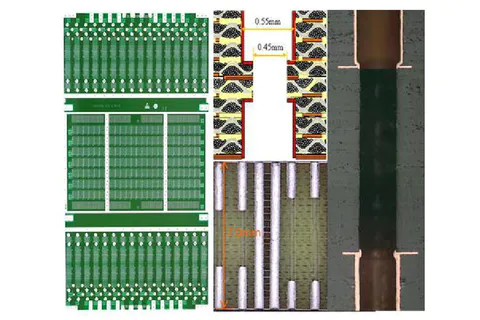
The dual-drilling, also known as forward and reverse drilling pcb, is a two-sided step-by-step drilling method. The first drilling is depth-controlled drilling, and the second drilling is through-hole drilling. Because the same through hole is completed by two drilling holes, it needs two drilling locations, so the design requirements of drilling locations are very high! Usually, because the location design is unreasostepable or the size design of the two drilling tools is unreasonable, there will be a "step hole" defect, which will have a fatal impact on the press-fit device in PCB assembly.
The number of PCB backplane row jacks is very large, It takes twice drills to complete the through hole processing
The design of dual-drilling positioning hole
Conventional drilling positioning holes are generally designed as three, but for dual-drill, need to change the orientation of drilling, the alignment of two drilling holes is very high. In the initial stage of this kind of board processing, in order to facilitate operation and reduce the error caused by the switching of the front and back drills, we designed four positioning holes for positioning. The advantages of the design of the positioning hole are that after the first depth control drilling, the pin hole need not be drilled again, only need to reload the board in reverse, which can eliminate the errors caused by the two positioning pins. However, the processing results show that there are still "step holes" in the four-hole positioning processing.
In order to reduce the "step hole" defect, we use a drilling positioning method called "over-positioning". For dual drilling, only X and Y directions need to be considered. The positioning method is: six positioning holes are designed, and six positioning holes are symmetrical in the center of the board.
Determination of dual-drill drilling tool difference
Front depth control drilling, and then reverse drilling, two drilling can not be the same size, after testing, depth control drilling tool is 0.2 mm or 0.3 mm smaller than through-hole drilling tool. Generally, the finished row hole size of PCB backplane is 0.6mm (24mil). If the difference is too big, the depth control drill tool is too small, and the processing difficulty is increased.
Determination of drilling processing sequence
It is customary for us to drill the hole with the component side up and then drill the hole with the solder side up. Later, it was found that once the bad step hole appeared in the processing, it would make the pressing joint not firm and lead to bad electrical contact. Because the slots are inserted from the component surface, if the "step hole" is produced, the upper half of the PIN needle can not be well fixed.
In order to prevent the occurrence of "step holes" from affecting the press-fit device, the correct processing sequence for drilling technology should be as follows: first, the solder side is controll depth drilling upward, and then drilling through hole with component side up.
Conclusion
PCB backplane dual-drilling technology is an effective way to improve the quality of thick PCB backplane drilling. The drilling positioning method and drilling sequence described in this paper are the key factors in this process. Because the drilling is completed twice, the disadvantage of this method is that it reduces the efficiency of drilling, and has a high requirement for the alignment ability and depth control ability of the drilling machine. PCB backplane dual-drilling technology is an effective means to solve the problem of high thickness PCB backplane drilling.
QUICK LINKS
CONTACT US
Office: (+86) 755 23040566
Tel: (+86) 158 9965 5195
E-mail: sales@rocket-pcb.com
Skype: Hans@Rocket-PCB
Whatsapp: 86 1589965 5195
Office Address: 301 Building/B, Huafeng Digital Technology Industrial Park, Chaoyang Ro, Yanchuan, Songgang,518105 Shenzhen, China.
Plant ADD.: No 69, Lianfeng North Road, Xianxi Area, ChangAn Town, Dongguan, China.


