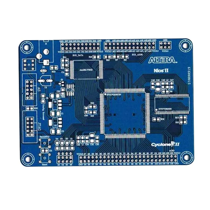
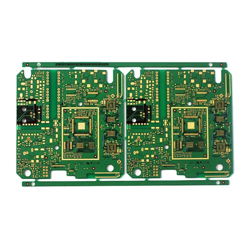
A common fault analysis multilayer circuit board
by:Rocket PCB
2020-07-04
Double-sided circuit board is the middle layer medium, both sides are walking the line layer.
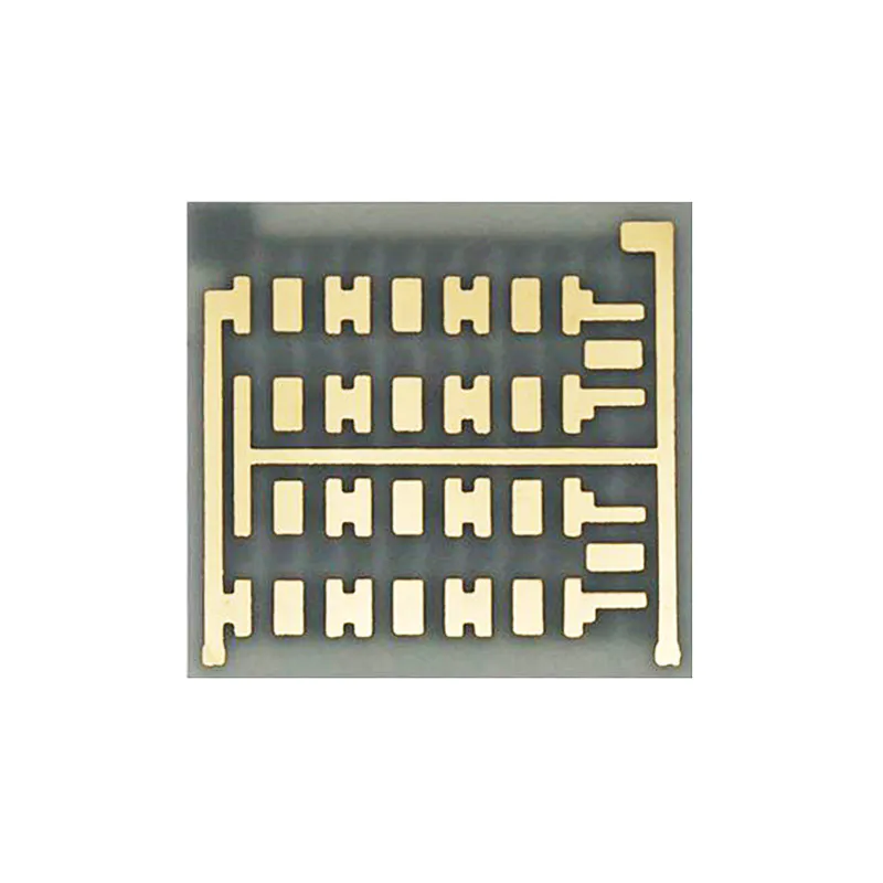
Multilayer circuit board is multilayer wire layer, each is between two layers of dielectric layer, can be done very thin dielectric layers.
Multilayer circuit boards at least three conductive layer, two layer surface, and the rest of the layer were synthesized in insulation board.
The electrical connection between them is usually through cross circuit board plated through hole.
In a series of production process in PCB, matching point many, carelessly the board is defective, inescapably, PCB quality problems will emerge in endlessly.
So after forming in production of circuit boards, tests will become an indispensable link.
Here to share with you about the failure of PCB and its solving measures.
A, multilayer circuit board often occurs in the use of which layer 1.
Supplier material or process problems;
2.
Improper packing or saved, be affected with damp be affected with damp;
3.
Poor design material selection and the surface of the copper distribution;
4.
Save the time is too long, more than the shelf life, PCB be affected with damp be affected with damp.
Response: choose good packaging, the use of constant temperature and humidity equipments for storage.
Completes the PCB factory reliability test, such as: PCB thermal stress test of reliability tests, responsible for the supplier is more than five times stratification as the standard, in the sample stage and mass production of each cycle for confirmation, and general circuit board manufacturers may require only 2 times, and a few months will only be confirmed once.
And the IR test of simulated SMT also can prevent bad product outflow, more is good PCB factory is necessary.
In addition, the PCB board Tg to choose above 145 ℃, such ability is safe.
Reliability test equipment: constant temperature and humidity box, stress screening type cold heat shock test chamber, PCB reliability test special equipment.
Multilayer circuit board production 2 for PCB, multilayer PCB soldering of bad reason: place time is too long, lead to moisture absorption, the layout is contaminated, oxidation, black nickel is abnormal, anti welding SCUM (
Shadow)
, the welding PAD.
Solution: when the choose and buy should pay close attention to PCB factory strictly quality control plan and the maintenance of the standards set.
Black nickel, for example, needs to see outgoing circuit board manufacturers have the gold, the gold thread potions concentration is stable, the analysis of frequency enough, whether to set up a regular stripping gold test and test to detect phosphorus content, internal soldering test whether there is a good execution, etc.
Three, multilayer circuit board impedance bad reasons: PCB impedance difference between batches is larger.
Response: for PCB manufacturers to ship the batch test report and impedance, when necessary to provide plate inside diameter and diameter of comparative data between the lines.
Four, multilayer PCB plate bending plate up reason: supplier selection is not reasonable, heavy industry control bad, improper storage, pipelining is unusual, the layers of copper area difference to be markedly, broken hole production were not strong enough, and so on.
Response: wrap sheet pressurized with wood pulp board before shipment, in order to avoid after deformation, when it is necessary to add the fixture on the patch to prevent bending board device is overweight.
PCB before packaging need to simulate IR loading condition experiment, so as not to appear after the furnace plate is bent.
Five, prevent weld blister/loss reasons: prevent welding ink selection have differences, multilayer circuit board welding process is abnormal, caused heavy or patch temperature too high.
Response: PCB suppliers to develop the reliability of the multilayer circuit board testing requirements, control in the different production processes.
Six, a tiffany effect reasons: in the OSP and daikin electronic dissolve for copper ions on the flow process lead to appear value for the difference between gold and copper.
Response: need circuit board manufacturers pay close attention to in the production process control of the potential difference between a gold and copper.
The use and installation of pcb making service is compared with most other systems for managing the pcb manufacturing services effectively and no doubt pcb making service have won the race so many times.
If you are looking for a reputable pcb making service pcb manufacturing services, you are on the lucky side as we are among the leading supplier in China. Visit the given links Rocket PCB to know more.
Through our distribution and marketing competencies, Rocket PCB Solution Ltd. provides creative, customized, solutions for our customers. As a result, we achieve superior profit growth as the pcb making service company of choice.
Your co-workers, investors and clients have busy schedules, and it can be hard to get everyone in the same place at the same time for pcb making service. So, it is important to create a connection between company and clients.
Custom message