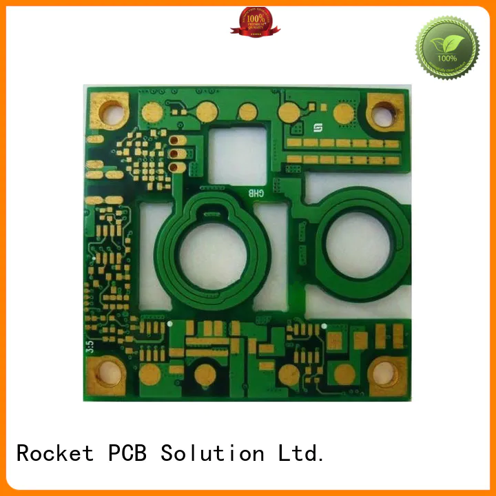


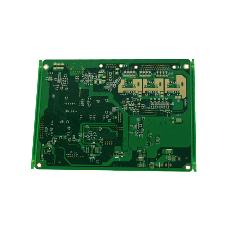
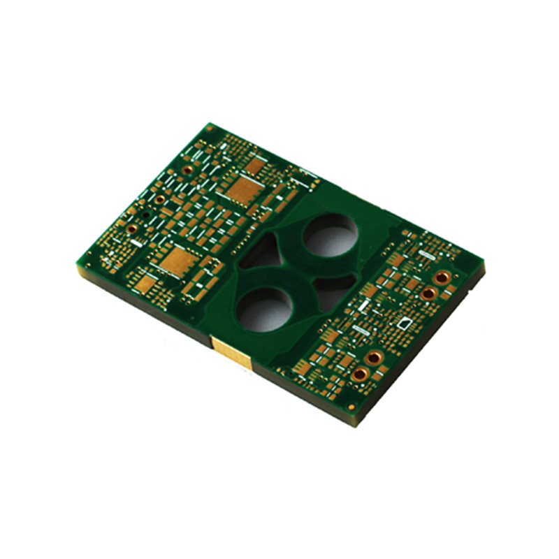
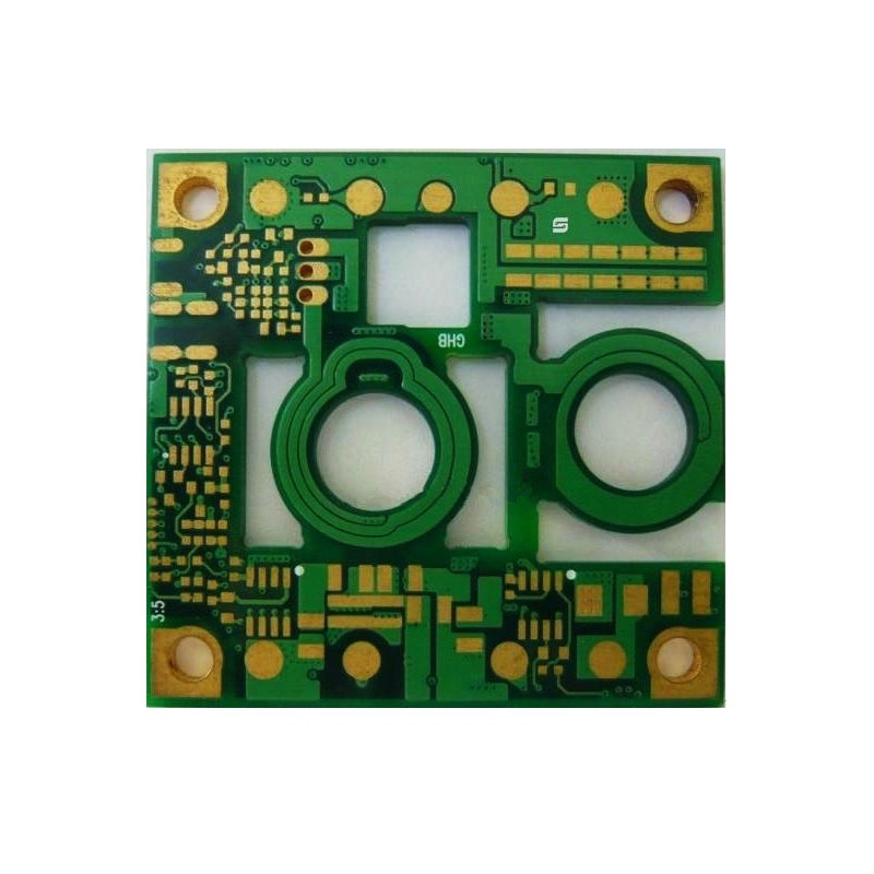
Thick copper board, refers to the circuit board whose inner layer base copper or outer layer finished copper thickness ≥2oz. Used to carry large current, reduce thermal strain and heat dissipation, mostly used in communications equipment, aerospace, automotive, network energy, planar transformers and power modules, etc.
With the more and more integrated chip technology, the circuit board is also constantly moving towards a light, thin, short, small direction, etching line width is getting smaller, but the current on the line needs to be carried more and more large.Therefore, the requirement for copper thickness is also increased to 102.9μm (30z), 137.2m (4oz), even 171.5um 50z), 205.7μm (60z)
In the etching process, fresh etching solution is difficult to enter due to the thick copper; the pool effect is obvious.Then due to its own equipment capacity (etching process capacity) limitations, thick copper etching is often a difficult process.There are many factors affecting etching, Rocket PCB through many years of experience in the manufacture of thick copper, for different copper thickness, different lines of design, different etching methods, Here are some of our experiences.
1, When the thick copper board is etched, a more uniform etching line (linear) and etching factor can be obtained by alternating etching without changing the production conditions
2, Multiple etching is equivalent to an increased etching capacity, that is, a line that can be etched to a smaller spacing relative to a single etching.
3, When the thick copper is etched, the direction of the dense line length is used as the etching direction, and better etching factors and lines (linear) can be obtained.
4. Etching factor = etching line thickness/[downline width-online width)/2]; It has reference value as etching quality standard when thick copper etching.








Copyright © 2026 Rocket PCB Solution Ltd. | All Rights Reserved Sitemap Friendship link: CNC machining heat sink