loading
Rocket PCB  >  AI - Page Sitemap  >  hybrid rf applications material structure for digital product
hybrid rf applications material structure for digital product

hybrid rf applications material structure for digital product
  • hybrid rf applications material structure for digital product
  • hybrid rf applications material structure for digital product
  • hybrid rf applications material structure for digital product

hybrid rf applications material structure for digital product

The design of Rocket PCB rf applications has been optimized. For example, the system components including geometric stress of the parts, the flatness of section, and connection mode have been improved by our designers.
Inquire Online
Get the latest price
Quantity Needed:
Pieces
E-mail:

hybrid rf applications material structure for digital product-1
hybrid rf applications material structure for digital product-2

hybrid RF PCB


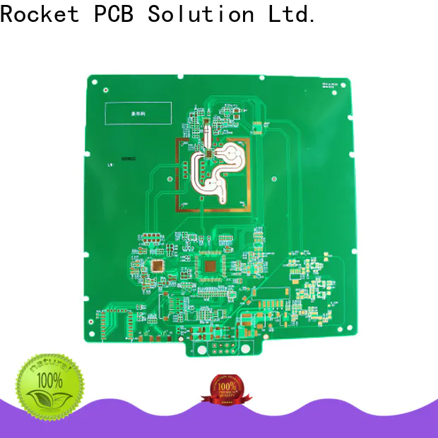
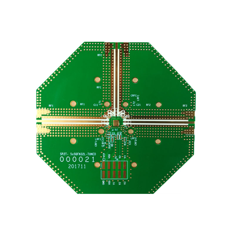
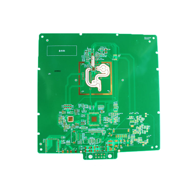
Because it is a high frequency signal transmission, the characteristic impedance of the finished printed board wire is required to be strict, and the line width of the board usually requires ±0.02mm. Therefore, the etching process needs to be strictly controlled, and the negatives used for optical imaging transfer should be compensated according to the line width and copper foil thickness.
The lines of such printed boards do not transmit current, but high-frequency electrical pulse signals, and defects such as pits, notches and pinholes on the wires affect transmission, and any such minor defects are not allowed. Sometimes, the thickness of the soldermask will also be strictly controlled, too thick or too thin soldermask on the line which a few microns will also be judged unqualified.
Thermal shock 288℃,10 seconds, 1~3 times, no hole wall separation.

For PTFE plate, to solve the wetting in the hole, there is no cavity in the PTH, the copper layer electroplated in the hole to withstand thermal shock, which is one of the difficulties in making the Teflon board


Where is the high frequency Hybrid board used


Satellite receivers, base antennas, microwave transmissions, automotive telephones, global positioning systems, satellite communications, communication equipment connectors, receivers, signal oscillators, home appliances networking, high-speed running computers, oscilloscopes, IC test instruments, etc., high-frequency communications. Frequency communication, high-speed transmission, high confidentiality, high transmission quality, high memory capacity processing and other communications and computer fields need high-frequency microwave printed boards


Product application


hybrid rf applications material structure for digital product-3                
Consumer electronics
hybrid rf applications material structure for digital product-4                
Automotive electronics
hybrid rf applications material structure for digital product-5                
Communications
hybrid rf applications material structure for digital product-6                
Energy
hybrid rf applications material structure for digital product-7                
Industrial & Instrumentation
hybrid rf applications material structure for digital product-8                
IOT/Smart Home
hybrid rf applications material structure for digital product-9                
Medical electronics
hybrid rf applications material structure for digital product-10                
Security Industry

Rocket PCB rf applications has to go through diverse tests. These tests include fatigue resistance testing, dimensional stability testing, chemical resistance testing, and mechanical testing.
Rocket PCB rf applications is a fruit of various subjects knowledge. It adopts CNC technology, power machinery, mechanical engineering and technology, tribology, thermodynamics, and others during its development stages.
The materials of Rocket PCB rf applications have been tested to meet the expected mechanical performance. Its strength, ductility, and toughness have been tested.
During the quality inspection of Rocket PCB rf applications, different inspecting approaches will be adopted. It will be checked by visual examination, radiographic inspection, or magnetic crack detection.
The manufacture of Rocket PCB rf applications requires the use of different facilities. It is processed under stamping, coating, painting, and drying equipment that features high performance and efficiency.
rf applications Excellent selection of materials, fine workmanship, high quality, and long-term use will not cause blistering, peeling, or cracking.
Product Message
Chat Online
Chat Online
Leave Your Message inputting...
Thank you for your attention. Please kindly describe your question first, or please send your inquiry to our email sales@rocket-pcb.com, and we will reply to you ASAP. Welcome, what can I help you?
Sign in with: