Easily learn the PCB design specifications
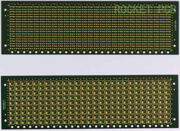
As a pretend bility, pursue the PCB engineers, how to draw a neat, efficient and figure of PCB? PCB design seemingly complex, both want to consider a variety of signals and concerns to the direction of the energy transfer, interference of fever and fret and always follow you. In fact, as long as the PCB design specifications are very clear to sum up, namely 'how to set' and 'how'. How to put 1, follow the 'first after small, difficult before they are easy' layout principle, namely important unit circuit, core components shall give priority to layout. This a buffet and truth is the same: buffet appetite is limited to anything like the first, PCB space is limited to pick important place. Easy to learn after the first big small PCB design specification, difficult before they are easy 2, heating element to generally should be evenly distributed, facilitate veneer and heat dissipation of the engine, in addition to the temperature detecting element temperature sensitive device should be far away from the heat of large components. 3, the arrangement of components to facilitate debugging and maintenance, i. e. small components cannot be placed around the big components, need to debug the components to have enough space around, too crowded situation tends to get very embarrassed. Fever uniform distribution 4 components were distributed evenly heating components, layout should be reference principle block diagram, main components according to the arrangement of the main signal flow regularity of veneer. Layout should meet the following requirements: general wire as short as possible, the shortest signal lines; The layout of the decoupling capacitor as far as possible close to the IC power supply pins, and make it with the power and ground loop is formed between the shortest; Reduce the signal to run to success, to prevent an accident on the road. Part five, the structure of the same circuit, as far as possible, use 'symmetric' standard layout; According to the uniform distribution, center of gravity balance standard optimization layout, layout is beautiful. 6, with the type of instrumentation components in X or Y direction should be placed in one direction. The same type of polar discrete component will also strive to be consistent in X or Y direction, facilitate production and inspection. 7, high voltage, high current signals and low current, low voltage is completely separated from the weak signal; Analog signal and digital signal separately; High frequency signal is separated from low frequency signal; The high frequency components are fully. Component layout, should be appropriate to consider using the same kind of power supply devices together, as far as possible for future power separating. How even how 'place' is the layout of the main points for attention, and 'why' is relatively more complicated, in general is: 1, the priority rules: if there are rules, arrangement will be the priority rules require signal lines, then decorate non-critical signal lines; 2, the key signal priority: power supply, analog signal, high speed signal, the clock signal, differential signal and synchronization signals such as the key priority wiring; 3, density priority: connection to the most complex components from the veneer to wiring, starting from the attachment the most densely populated area on a single board wiring. PCB layout sample PCB layout example intelligent people are good at making complex things simple, you learn how 'pendulum' and 'why', PCB design specification soeasy!