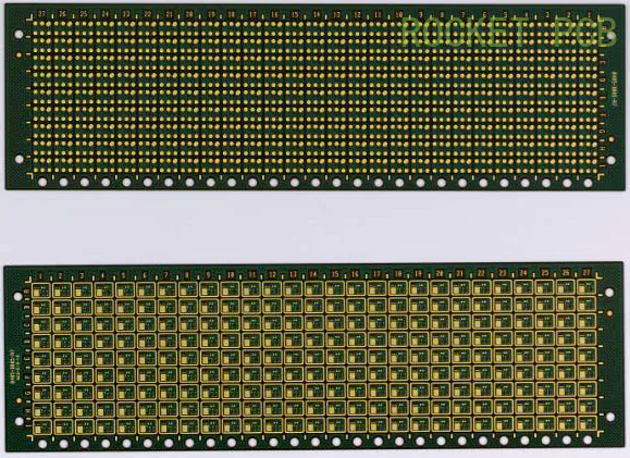
Chongqing SMT, sample patches, medium and small batch - SMT solder processingPoly (ding SMT processing factory
As PCB board factory system often encounter some purchasing PCB purchasing find we struggle to tell us: their PCB engineers design a lot of PCB board manufacturers make uncertain.
General board manufacturer can't do it, and as a procurement generally do not understand technology, also don't know the PCB manufacturing process, don't know how to communicate with PCB board factory system, I couldn't put the PCB designer's idea, so as to get effective improvement Suggestions.
Here, the first response is to let them send me the drawings, our little brother/sister to you in person, see which way PCB design and send out again?
Look at the (
PCB laminated)
Drawings after found, it is a familiar old driver, can only say that many designers did not understand the PCB factory manufacturing process!
Point 1 below clap clap a problem.
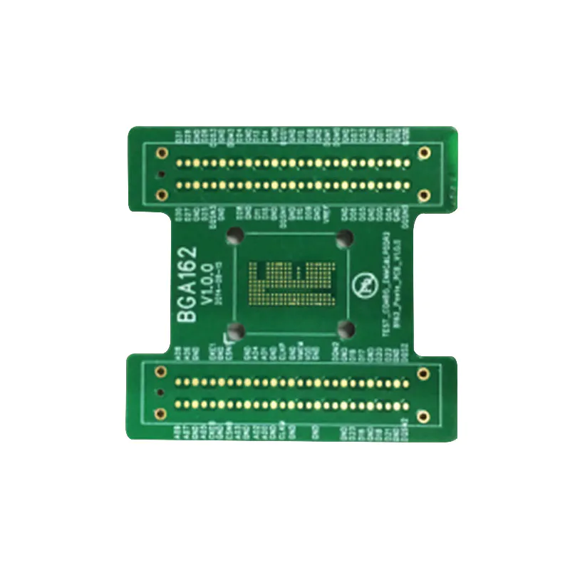
The BGA chip centre spacing is 0.
4 mm, and the design engineer in design between BGA solder line.
2.
Design the circuit board between multiple BGA solder hole.
Next to brother said under MAO PCB board factory to see such a design, system could not be made 1, BGA from its 0.
Minimum 4 mm, BGA be 0.
2 mm, BGA welding plate spacing is only 0.
2mm。
If go line, line is the limit of the minimum 3 mil, namely zero.
075mm。
As a result, the line only: (the distance to the welding plate
0.
4 -
0.
2 -
0.
075).
÷2=0.
0625 mm, only 2.
46mil。
The spacing between the PCB factory engineer will say do your younger sister!
On: dry goods, give you brother emphasized the two extreme limit range 1, PCB production BGA line of minimum 3 mil, BGA line to the bonding pad spacing minimum 3 mil.
2, via any graphics (
Line, the welding plate, copper)
The limit distance: outer limit distance: 6 mil.
Circuit board lining distance limit: 8 mil.
So someone will ask: for fur lining distance larger than the outer requirements?
Because in the process of PCB production, the inner pressing registration deviation will be bigger!
Here, the design engineer should force a face of meng: zero today.
2 mm of BGA chip, more and more, can't we have the solution?
Answer is certainly yes, must have!
With the advent of intelligent, electronic device is more and more precise, these are must solve the problem!
Next to tell me the solution design plate hole, brother walk resin plug hole process!
Plate hole, just as its name implies is that on the welding plate punch!
Exactly how to plate hole of a PCB production process?
Here is a detailed introduction of!
Hole plate manufacturing process including: drilling, plating, resin plug hole, baking and grinding.
First of all, drilling here are generally play laser drilling hole.
Mechanical hole limit minimum drill to 0.
15 mm, if it is zero.
1 mm hole, you must use the laser perforation to drill.
After drilling the hole to hole metallization electroplating, then used resin plug hole, after baking is grinding grinding of flat and smooth after the resin because do not contain copper, but again a layer of copper on it into a PAD, the process is in the original PCB drilling system before, is the first fort hole hole processing good, then other holes, according to the normal PCB factory process.
The general PCB design plate hole of the board will be mentioned in the blind or buried holes, such as a (
PCB laminated)
Four layer board: 1 layer -
—
Layer 2 plate hole, then layer 2 -
—
1 layer go line up, then 1 layer -
—
4 layer can also punch line.
This formed a 1 -
2, 1
4 or 1 -
2, 1
4, 3 -
4 the four layers of first-order HDI board.
Of course,
PCB laminated)
Europebecame layer board can also be the same design, like a conventional drill with design order HDI board.
The above content by: :To provide the reference for you!
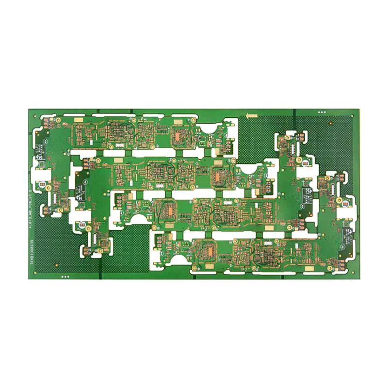
Rocket PCB Solution co Ltd is a professional: PCB manufacture manufacturer, to provide you with: PCB proofing, batch plate, 1 -
34 layer PCB board, high TG board, impedance board, HDI board, Rogers plate, microwave plate, radio frequency (rf) board, LeiDaBan, thick copper foil board, such as PCB manufacturing production of various kinds of technology and material.
Welcome to consult customer service for more details.
In the present growing world of emerging technology, the has demanding operation in various sectors like pcb manufacturing services, pcb manufacturing services, pcb manufacturing services and many other industries at pcb manufacturing services levels of manufacturing and designing.
Deliver value to our customers by providing the most reliable and efficient products as pcb service.
Rocket PCB Solution Ltd. believes that the shorter the path between consumer and product, the more likely businesses are to convert more sales.